

NTE NTE6409 Datasheet

NTE6409
Unijunction Transistor
Description:
The NTE6409 is designed for use in pulse and timing circuits, sensing circuits and thyristor trigger
circuits.
Features:
D Low Peak Point Current: 2µA Max
D Low Emitter Reverse Current: 200nA Max
D Passivated Surface for Reliability & Uniformity
Absolute Maximum Ratings: (TA = +25°C, unless otherwise specified)
Power Dissipation (Note 1), PD 300mW. . . . . . . . . . . . . . . . . . . . . . . . . . . . . . . . . . . . . . . . . . . . . . . . . . .
RMS Emitter Current, I
E(RMS)
50mA. . . . . . . . . . . . . . . . . . . . . . . . . . . . . . . . . . . . . . . . . . . . . . . . . . . . . .
Peak Pulse Emitter Current (Note 2), iE 2A. . . . . . . . . . . . . . . . . . . . . . . . . . . . . . . . . . . . . . . . . . . . . . . .
Emitter Reverse Voltage, V
Interbase Voltage, V
35V. . . . . . . . . . . . . . . . . . . . . . . . . . . . . . . . . . . . . . . . . . . . . . . . . . . . . . . . . . .
B2B1
B2E
30V. . . . . . . . . . . . . . . . . . . . . . . . . . . . . . . . . . . . . . . . . . . . . . . . . . . . . .
Operating Junction Temperature Range, TJ –65° to +125°C. . . . . . . . . . . . . . . . . . . . . . . . . . . . . . . . .
Storage Temperature Range, T
–65° to +150°C. . . . . . . . . . . . . . . . . . . . . . . . . . . . . . . . . . . . . . . . . .
stg
Note 1. Derate 3mW/°C increase in ambient temperature. The total power dissipation (available
power to Emitter and Base–Two) must be limited by the external circuitry.
Note 2. Capacitor discharge: 10µF or less, 30V or less
Electrical Characteristics: (TA = +25°C unless otherwise specified)
Parameter Symbol Test Conditions Min Typ Max Unit
Intrinsic Standoff Ratio η V
Interbase Resistance r
Interbase Resistance
αr
BB
BB
= 10V, Note 3 0.68 – 0.82
B2B1
V
= 3V, IE = 0 4.7 7.0 9.1 kΩ
B2B1
V
= 3V, IE = 0, TA = –55° to +125°C 0.1 – 0.9 %/°C
B2B1
Temperature Coefficient
Emitter Saturation Voltage V
Modulated Interbase Current I
Emitter Reverse Current I
EB1(sat)VB2B1
B2(mod)VB2B1
EB2O
Peak Point Emitter Current I
Valley Point Current I
Base–One Peak Pulse
V
P
V
OB1
= 10V, IE = 50mA, Note 4 – 3.5 – V
= 10V, IE = 50mA – 15 – mA
V
= 30V, IB1 = 0 – 0.005 0.2 µA
B2E
V
= 25V – 1 2 µA
B2B1
V
= 20V, RB2 = 100Ω, Note 4 8 10 18 mA
B2B1
Voltage
Note 3. Intrinsic Standoff Ratio, η, is defined by the equation:
VP – V
η =
V
F
B2B1
Where: VP = Peak Point Emitter Voltage
V
= Interbase Voltage
B2B1
VF = Emitter to Base–One Junction Diode Drop ([ 0.45V @ 10µA)
6 7 – V
Note 4. Use pulse techniques: PW [ 300µs, Duty Cycle ≤ 2% to avoid internal heating due to inter-
base modulation which may result in erroneous readings.
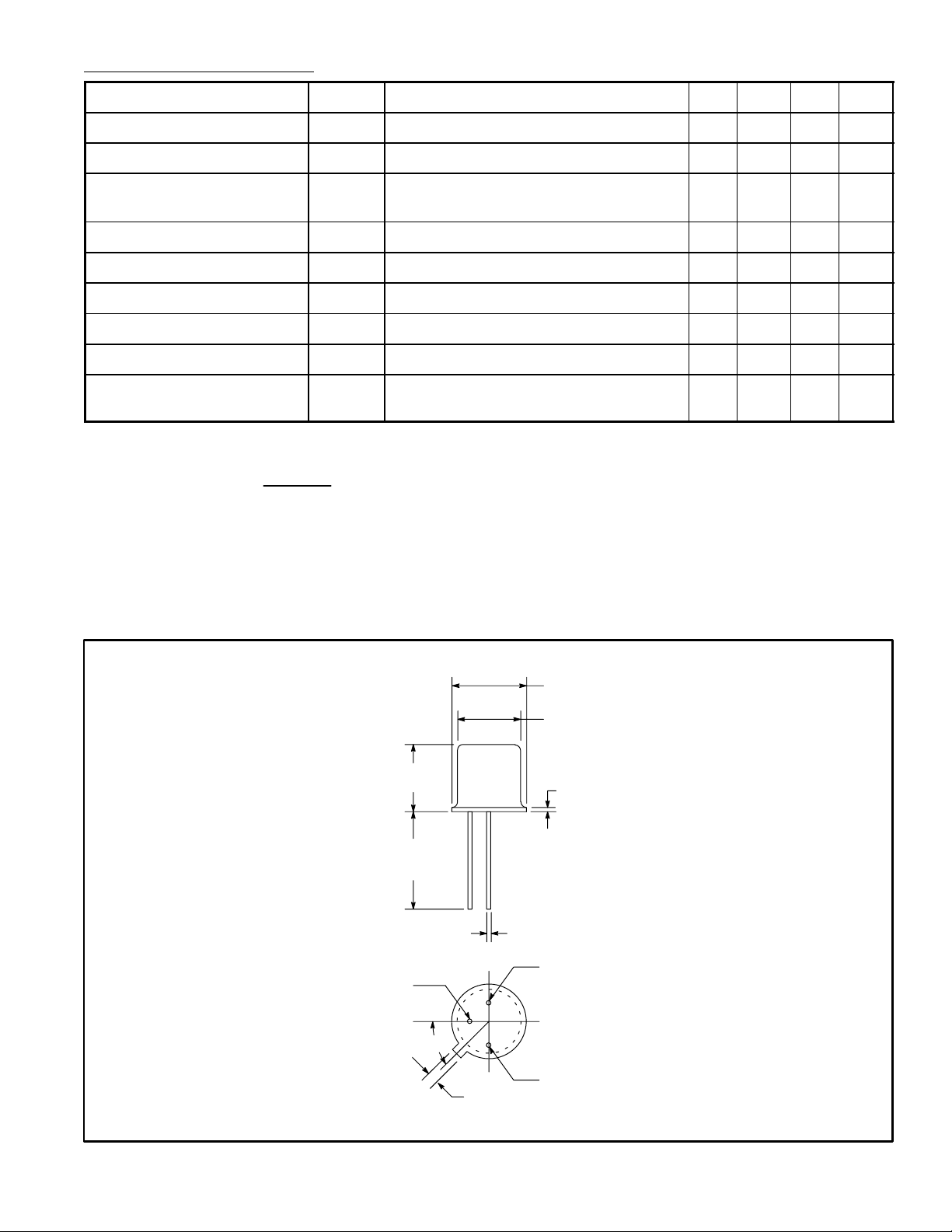
.230 (5.84) Dia Max
.195 (4.95) Dia Max
.210 (5.33)
Max
.500
(12.7)
Min
.018 (0.45)
Emitter
45°
.030 (.762) Max
Base 1
.041 (1.05)
Base 2/Case
 Loading...