

NTE NTE6403 Datasheet
NTE6403
Integrated Circuit
Silicon Bilateral Switch (SBS)
Description:
The NTE6403 is a silicon planer, monolithic integrated circuit having the electrical characteristics of
a bilateral thyristor . This device is designed to switch at 8 volts with a 0.02%/°C temperature coefficient and excellently matched characteristics in both directions. A gate lead is provided to eliminate
rate effect and to obtain triggering at lower voltages.
The NTE6403 is specifically designed and characterized for applications where stability of switching
voltage over a wide temperature range and well matched bilateral characteristics are an asset. It is
ideally suited for half wave and full wave triggering in low voltage SCR and TRIAC phase control circuits.
Absolute Maximum Ratings: (TA = +25°C unless otherwise specified)
Peak Recurrent Forward Current (PW = 10µs, Duty Cycle = 1%, TA = +25°C) 1A. . . . . . . . . . . . . . .
Peak Non–Recurrent Forward Current (PW = 10µs, TA = +25°C) 5A. . . . . . . . . . . . . . . . . . . . . . . . . .
Power Dissipation (Note 1), P
D
DC Forward Anode Current (Note 1) 175mA. . . . . . . . . . . . . . . . . . . . . . . . . . . . . . . . . . . . . . . . . . . . . . .
DC Gate Current (Note 1, Note 2) 5mA. . . . . . . . . . . . . . . . . . . . . . . . . . . . . . . . . . . . . . . . . . . . . . . . . . .
Operating Junction Temperature Range, T
Storage Temperature Range, T
stg
J
–55° to +125°C. . . . . . . . . . . . . . . . . . . . . . . . . . . . . . . . . .
–65° to +150°C. . . . . . . . . . . . . . . . . . . . . . . . . . . . . . . . . . . . . . . . . .
Note 1. Derate linearly to zero at +125°C.
Note 2. This rating applicable only on OFF state. Maximum gate current in conducting state limited
by maximum power rating.
300mW. . . . . . . . . . . . . . . . . . . . . . . . . . . . . . . . . . . . . . . . . . . . . . . . . . . .
Electrical Characteristics: (TA = +25°C, Note 3 unless otherwise specified)
Parameter Symbol Test Conditions Min Typ Max Unit
Static
Switching Voltage V
Switching Current I
Absolute Switching Voltage Difference |VS2 – VS1| – – 200 mV
Absolute Switching Current Difference |IS2 – IS1| – – 10 µA
Holding Current I
OFF State Current I
Temperature Coefficient of Switching Voltage T
ON State Forward Voltage Drop V
Forward Gate Current to Trigger I
S
H
B
GF
S
VF = 5V TA = +25°C – – 0.1 µA
TA = +85°C – – 10.0 µA
C
F
TA = –55° to +85°C – ±0.05 – %/°C
IF = 175mA – – 1.7 V
VF = 5V, RL = 1kΩ – – 100 µA
7.5 – 9.0 V
– – 120 µA
– – .5 mA
Note 3. This d evice i s a s ymmetr ical n egative r esi stance d iode. All e lectr ical l imits s how n a bove a pply
in either direction of current flow.
Electrical Characteristics (Cont’d): (TA = +25°C, Note 3 unless otherwise specified)
Parameter Symbol Test Conditions Min Typ Max Unit
Dynamic
Peak Pulse Amplitude V
Turn–On Time t
Turn–Off Time t
o
on
off
3.5 – – V
– – 1.0 µs
– – 30.0 µs
Note 3. This d evice i s a s ymmetr ical n egative r esi stance d iode. All e lectr ical l imits s how n a bove a pply
in either direction of current flow.
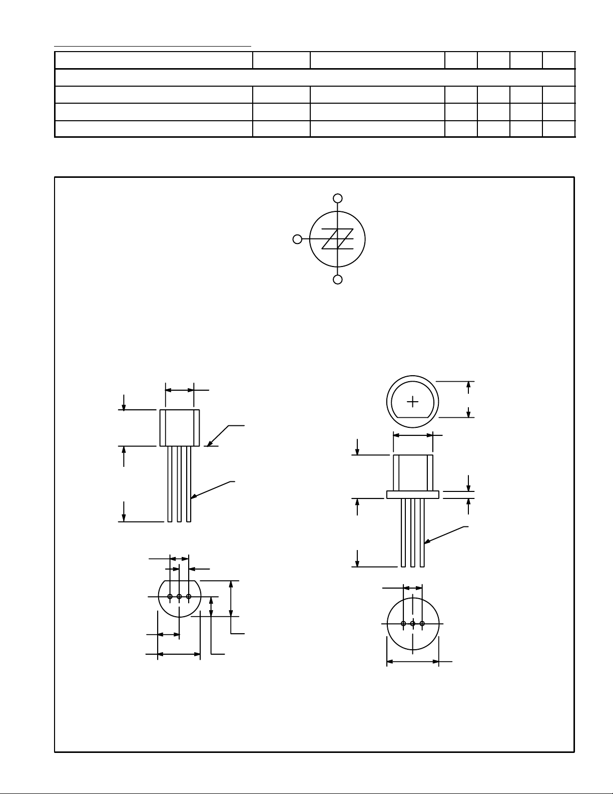
A
2
G
A
1
SBS CIRCUIT SYMBOL
.210
(5.33)
Max
.500
(12.7)
Min
.100 (2.54)
.105 (2.67) Max
.205 (5.2) Max
A1 G A
.135 (3.45) Min
2
.050 (1.27)
.105 (2.67) Max
Seating
Plane
.021 (.445)
Dia Max
.165 (4.2) Max
.245
(6.23)
Max
.500
(12.7)
Min
.100 (2.54)
A1 G A
.140 (3.55) Max
.190 (4.82) Min
.065
(1.65)
.018 (0.45) Dia Max
2
.200 (5.08) Max
 Loading...