

NTE NTE6401 Datasheet
NTE6401
Unijunction Transistor
Description:
The NTE6401 is designed for use in pulse and timing circuits, sensing circuits and thyristor trigger
circuits.
Features:
D Low Peak Point Current: 5µA (Max)
D Low Emitter Reverse Current: .005µA (Typ)
D Passivated Surface for Reliability & Uniformity
Absolute Maximum Ratings: (TA = +25°C unless otherwise specified)
Power Dissipation (Note 1), P
RMS Emitter Current, I
E(RMS)
Peak Pulse Emitter Current (Note 2), i
Emitter Reverse Voltage, V
Interbase Voltage, V
B2B1
D
E
B2E
Operating Junction Temperature Range, T
Storage Temperature Range, T
stg
J
–65° to 125°C. . . . . . . . . . . . . . . . . . . . . . . . . . . . . . . . . . .
–65° to +150°C. . . . . . . . . . . . . . . . . . . . . . . . . . . . . . . . . . . . . . . . . .
300mW. . . . . . . . . . . . . . . . . . . . . . . . . . . . . . . . . . . . . . . . . . . . . . . . . . . .
50mA. . . . . . . . . . . . . . . . . . . . . . . . . . . . . . . . . . . . . . . . . . . . . . . . . . . . . .
2A. . . . . . . . . . . . . . . . . . . . . . . . . . . . . . . . . . . . . . . . . . . . . . . .
30V. . . . . . . . . . . . . . . . . . . . . . . . . . . . . . . . . . . . . . . . . . . . . . . . . . . . . . .
35V. . . . . . . . . . . . . . . . . . . . . . . . . . . . . . . . . . . . . . . . . . . . . . . . . . . . . . . . . . . .
Note 1 Derate 3mW/°C increase in ambient temperature. The total power dissipation (available
power to Emitter and Base–Two) must be limited by the external circuitry.
Note 2 Capacitor discharge – 10µF or less, 30 volts or less
Electrical Characteristics: (TA = +25°C unless otherwise specified)
Parameter Symbol Test Conditions Min Typ Max Unit
Intrinsic Standoff Ratio
Interbase Resistance r
Interbase Resistance Temperature
Coefficient
η
BB
ar
BB
V
= 10V, Note 3 0.56 – 0.75 –
B2B1
V
= 3V, IE = 0 4.7 7.0 9.1 kΩ
B2B1
0.1 – 0.9 %/°C
Note 3. Intrinsic standoff ratio, η is defined by equation:
η = VP – V
V
F
B2B1
where VP = Peak Point Emitter Voltage
V
= Interbase Voltage
B2B1
VF = Emitter to Base–One Junction Diode Drop (∼ 0.45V @ 10µA)
Electrical Characteristics (Cont’d): (TA = +25°C unless otherwise specified)
Parameter Symbol Test Conditions Min Typ Max Unit
Emitter Saturation Voltage V
Modulated Interbase Current I
Emitter Reverse Current I
Peak Point Emitter Current I
Valley Point Current I
Base–One Peak Pulse Voltage V
EB1(sat)VB2B1
B2(mod)VB2B1
EB20
P
V
OB1
= 10V, IE = 50mA, Note 4 – 3.5 – V
= 10V, IE = 50mA – 15 – mA
V
= 30V, IB1 = 0 – 0.005 12 µA
B2E
V
= 25V – 1 5 µA
B2B1
V
= 20V, RB2 = 100Ω 4 6 – mA
B2B1
3 5 – V
Note 4. Use pulse techniques: Pulse Width ~ 300µs, duty cycle ≤ 2% to avoid internal heating due
to interbase modulation which may result in erroneous readings.
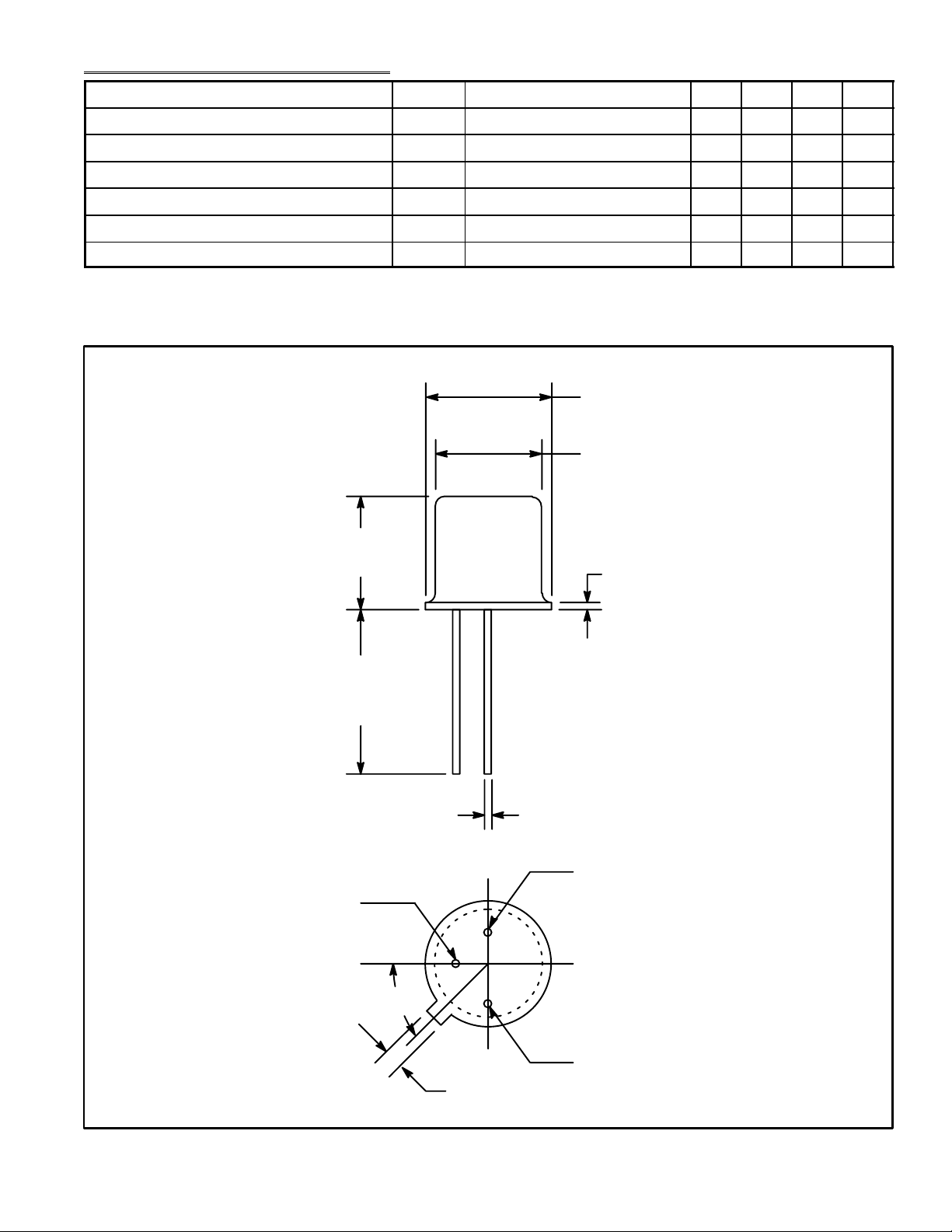
.230 (5.84) Dia Max
.195 (4.95) Dia Max
.210 (5.33)
Max
.030 (.762) Max
Emitter
.500
(12.7)
Min
.018 (0.45)
Base 1
45°
Base 2/Case
.041 (1.05)
 Loading...