

NTE NTE621 Datasheet

NTE621
Silicon Rectifier, General Purpose, High Voltage,
Standard Recovery
(Surface Mount)
Features:
D High Temperature Metallurgically Bonded
D Glass Passivated Junction
D High Temperature Soldering Guaranteed:
+450°C/5 Seconds at Terminals. Complete Device Submersible Temperature of
+260°C/10 Seconds in Solder Bath.
Maximum Ratings and Electrical Characteristics: (TA = +25°C unless otherwise specified.
60Hz, resistive or inductive load. For capacitive load, derate current by 20%.)
Maximum Recurrent Peak Reverse Voltage, V
Maximum RMS Voltage, V
Maximum DC Blocking Voltage, V
RMS
DC
Maximum Average Forward Rectified Current, I
Peak Forward Surge Current, I
FSM
(8.3ms Single Half Sine–Wave Superimposed on Rated Load) 30A. . . . . . . . . . . . . . . . . . . .
Maximum Instantaneous Forward Voltage (IT = 1A), V
Maximum DC Reverse Current (VDC = 400V), I
TA = +25°C 10µA. . . . . . . . . . . . . . . . . . . . . . . . . . . . . . . . . . . . . . . . . . . . . . . . . . . . . . . . . . . . . . . . .
TA = +125°C 50µA. . . . . . . . . . . . . . . . . . . . . . . . . . . . . . . . . . . . . . . . . . . . . . . . . . . . . . . . . . . . . . . .
Maximum Full Load Reverse Current (Full Cycle Average at TA = +75°C), I
Typical Junction Capacitance (Note 1), C
Operating Junction Temperature Range, T
Storage Temperature Range, T
stg
Maximum Thermal Resistance, Junction–to–Terminal (Note 2), R
Maximum Thermal Resistance, Junction–to–Ambient (Note 3), R
RRM
T(AV)
F
R
R(AV)
J
J
–65° to +175°C. . . . . . . . . . . . . . . . . . . . . . . . . . . . . . . . . .
–65° to +175°C. . . . . . . . . . . . . . . . . . . . . . . . . . . . . . . . . . . . . . . . . .
thJL
thJA
30°C/W. . . . . . . . . . . . . . . . . . .
75°C/W. . . . . . . . . . . . . . . . . . .
400V. . . . . . . . . . . . . . . . . . . . . . . . . . . . . . . . . . . . .
280V. . . . . . . . . . . . . . . . . . . . . . . . . . . . . . . . . . . . . . . . . . . . . . . . . . . . . .
400V. . . . . . . . . . . . . . . . . . . . . . . . . . . . . . . . . . . . . . . . . . . . . . . . .
1A. . . . . . . . . . . . . . . . . . . . . . . . . . . . . . . . . . . . .
1.1V. . . . . . . . . . . . . . . . . . . . . . . . . . . . . . . .
30µA. . . . . . . . . . .
15pF. . . . . . . . . . . . . . . . . . . . . . . . . . . . . . . . . . . . . . . . . . . .
Note 1. Measured at 1MHz and applied reverse voltage of 4VDC.
Note 2. Thermal resistance, junction–to–terminal, 6.0mm2 copper pads to each terminal.
Note 3. Thermal resistance, junction–to–ambient, 6.0mm2 copper pads to each terminal.
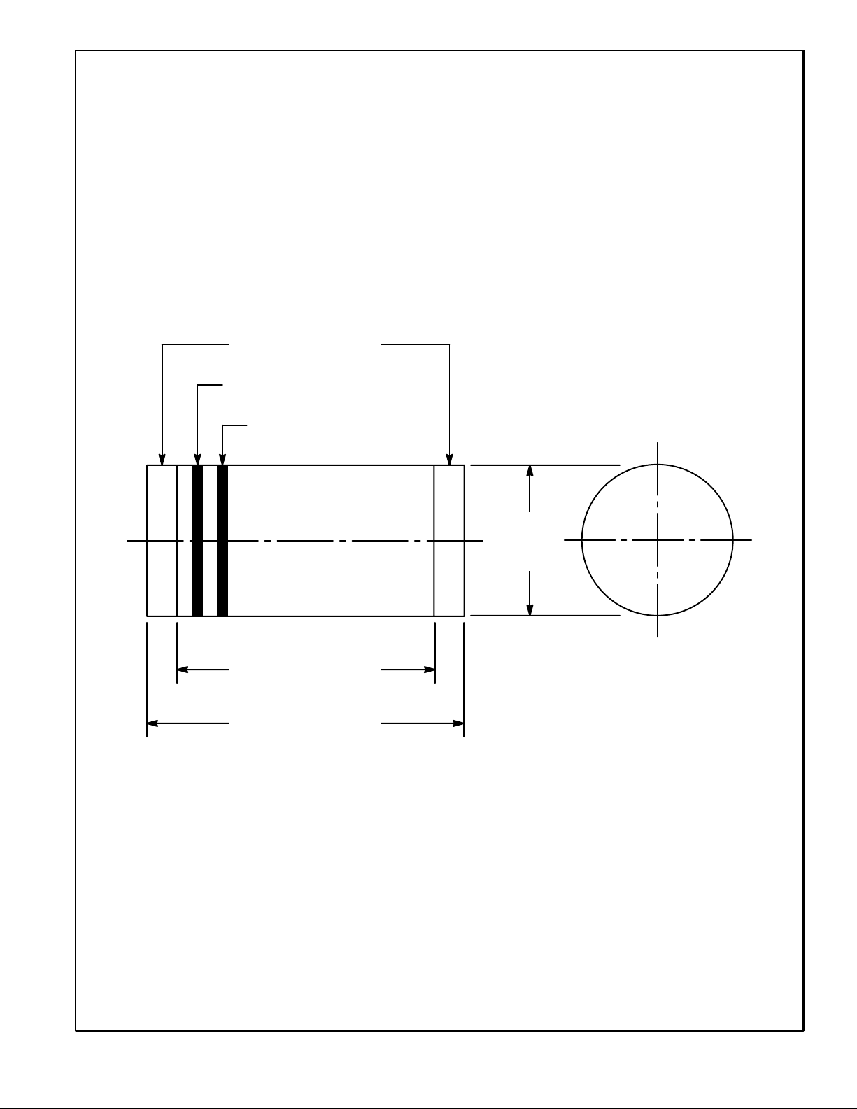
Solderable Ends
1st Band (Device Type)
2nd Band (Voltage Type)
.022 (.559) Max
.205 (5.207) Max
.105
(2.667)
Max Dia
Two Bands Indicates Cathode
 Loading...