

NTE NTE5661 Datasheet

NTE5661
TRIAC, 10 Amp
Description:
The NTE5661 is a TRIAC in a TO64 type stud mount package designed primarily for full–wave AC
control applications such as light dimmers, motor controls, heating controls, power supplies or wherever full–wave silicon gate controlled solid–state devices are needed. TRIAC type thyristors switch
from a blocking to a conducting state for either polarity of applied anode voltage with positive or negative gate triggering.
Features:
D Low “ON” Voltage
D Gate Triggering Guaranteed in Four Modes
Absolute Maximum Ratings:
Repetitive Peak Off–State Voltage (TJ = +100°C, Note 1), V
DRM
On–State RMS Current (TC = +75°C), ITRMS 10A. . . . . . . . . . . . . . . . . . . . . . . . . . . . . . . . . . . . . . . . . .
Peak Surge Current (One Full Cycle, 60Hz, TJ = –40° to +100°C), I
TSM
Circuit Fusing Considerations (TJ = –40° to +100°C, t = 1.0 to 8.3ms), I2t 40A2sec. . . . . . . . . . . . . .
Peak Gate Power, P
Average Gate Power, P
Peak Gate Current, I
Operating Junction Temperature Range, T
Storage Temperature Range, T
Thermal Resistance, Junction–to–Case, R
Thermal Resistance, Junction–to–Ambient, R
GM
GM
G(AV)
stg
J
thJC
–40° to +100°C. . . . . . . . . . . . . . . . . . . . . . . . . . . . . . . . . .
–40° to +150°C. . . . . . . . . . . . . . . . . . . . . . . . . . . . . . . . . . . . . . . . . .
thJA
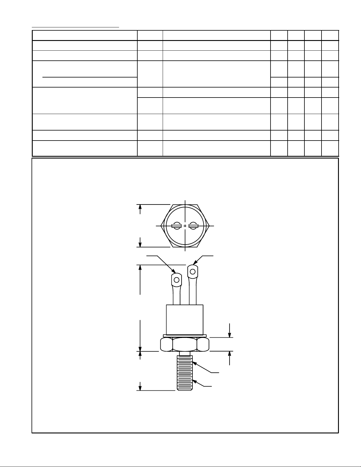
Stud Torque 15 in. lb.. . . . . . . . . . . . . . . . . . . . . . . . . . . . . . . . . . . . . . . . . . . . . . . . . . . . . . . . . . . . . . . . . . .
50V. . . . . . . . . . . . . . . . . . . . . . . . . .
100A. . . . . . . . . . . . . . . . . .
10W. . . . . . . . . . . . . . . . . . . . . . . . . . . . . . . . . . . . . . . . . . . . . . . . . . . . . . . . . . . .
0.5W. . . . . . . . . . . . . . . . . . . . . . . . . . . . . . . . . . . . . . . . . . . . . . . . . . . . . . . .
2A. . . . . . . . . . . . . . . . . . . . . . . . . . . . . . . . . . . . . . . . . . . . . . . . . . . . . . . . . . . . . .
2°C/W. . . . . . . . . . . . . . . . . . . . . . . . . . . . . . . . . . . . . . .
50°C/W. . . . . . . . . . . . . . . . . . . . . . . . . . . . . . . . . . . .
Note 1. Ratings apply for open gate conditions. Thyristor devices shall not be tested with a constant
current source for blocking capability such that the voltage applied exceeds the rated blocking voltage.
Electrical Characteristics: (TC = +25°C unless otherwise specified)
Parameter Symbol Test Conditions Min Typ Max Unit
Peak Blocking Current (Either Direction) I
On–State Voltage (Either Direction) V
Gate Trigger Current, Continuous DC
All Modes
DRM
I
V
= 50V, TJ = +100°C, Gate Open – – 2.0 mA
DRM
TMITM
GT
= 14A Peak – 1.3 1.8 V
Main Terminal Voltage = 12V, RL = 100Ω – – 40 mA
MT2 (+), G (+); MT2 (–), G (–) – – 50 mA
Gate Trigger Voltage, Continuous DC V
V
Main Terminal Voltage = 12V, RL = 100Ω – 0.9 2.0 V
GT
Main Terminal Voltage = 50V, RL = 100Ω,
GD
0.2 – – V
TJ = +1 00°C
Holding Current (Either Direction) I
Main Terminal Voltage = 12V,
H
– – 30 mA
Gate Open, Initiating Current = 100mA
Turn–On Time t
Blocking Voltage Application Rate
dv/dt V
ITM = 14A, IGT = 100mA – 1.5 – µs
on
= 50V, TJ = +75°C, Gate Open – 5.0 – V/µs
DRM
at Commutation
.431
(10.98
Max
Gate
.855
(21.7)
Max
.453
(111.5)
Max
MT
1
.125 (3.17) Max
MT
2
10–32 UNF–2A
 Loading...