

NTE NTE4950, NTE4934, NTE4936, NTE4970, NTE4920 Datasheet
...
NTE4902 thru NTE4998
Surge Clamping, Transient Overvoltage Suppressor
Unidirectional
Description:
The NTE4900 series of silicon Transient Suppressors designed to protect voltage sensitive components from high energy voltage transients. Transient over voltage suppressor devices have become
very important as a consequence of their high surge capability, extremely fast response time, and low
incremental surge resistance (Rs).
Application:
The NTE4900 series has a peak pulse power rating of 1500 watts for one millisecond can protect integrated circuits, hybrids, CMOS, MOS, and other voltage sensitive components in a broad range of
applications such as telecommunications, power supplies, computers, automotive, industrial, and
medical equipment.
Absolute Maximum Ratings:
Peak Pulse Power Dissipation (TA = +25°C) 1500W. . . . . . . . . . . . . . . . . . . . . . . . . . . . . . . . . . . . . . . .
t
clamping
Operating and Storage Temperature –65°C to +175°C. . . . . . . . . . . . . . . . . . . . . . . . . . . . . . . . . . . . .
Forward Surge Rating 200 Amps, 1/20 Second at +25°C. . . . . . . . . . . . . . . . . . . . . . . . . . . . . . . . . . . .
Steady State Power Dissipation 5.0 W @ T1 = +25°C. . . . . . . . . . . . . . . . . . . . . . . . . . . . . . . . . . . . . .
(0 volts to BV Min) < 1 x 10–12 sec. . . . . . . . . . . . . . . . . . . . . . . . . . . . . . . . . . . . . . . . . . . . . . .
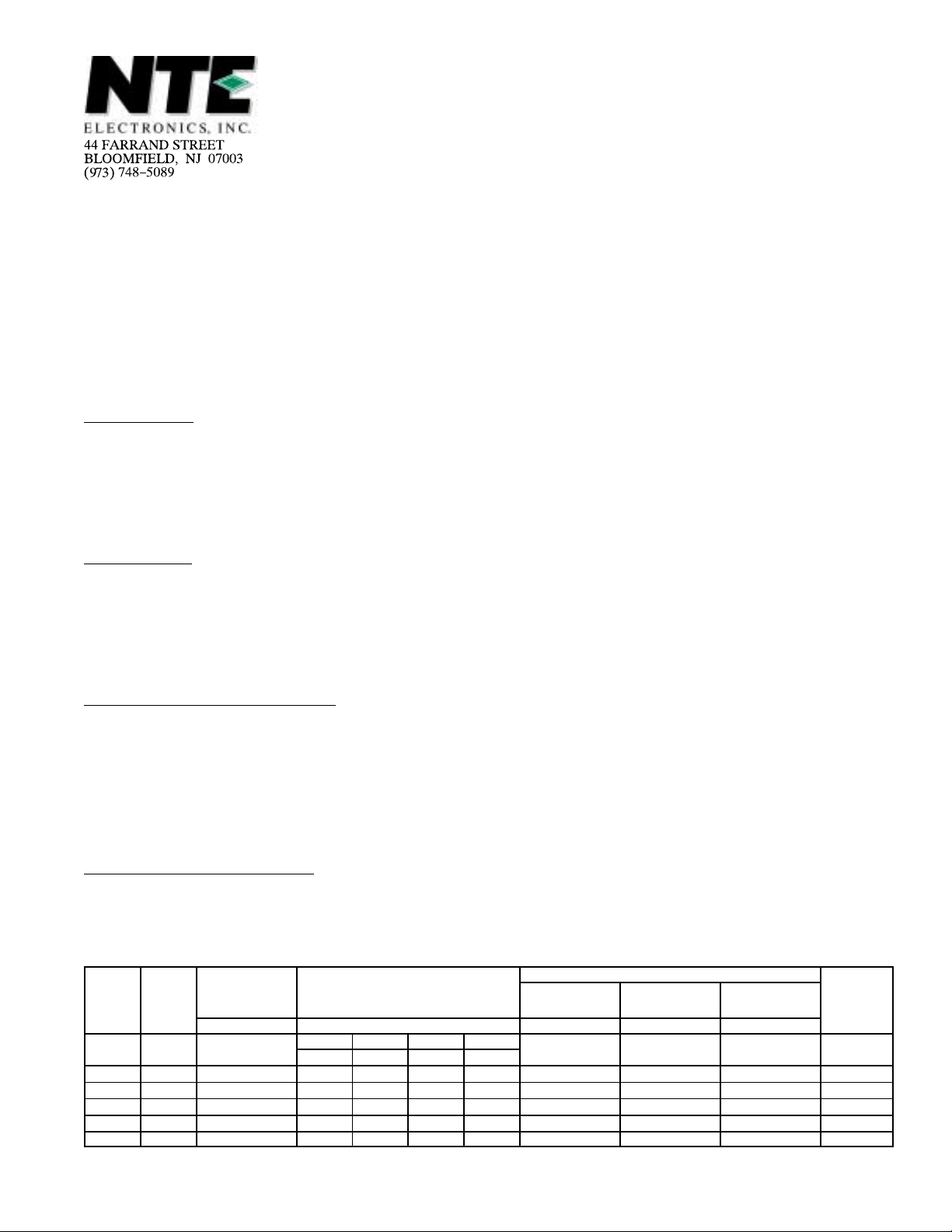
Electrical Characteristics:
Clamping Factor: 1.33 @ full rated power
1.20 @ 50% rated power
The clamping factor is defined as: The ratio of the actual V
(Clamping voltage) to the actual BV
C
(Breakdown Voltage) as measured on a specific device.
Maximum Ratings
Maximum Reverse
NTE Type
Number
4902 183 5.80 6.45 6.80 7.14 10.0 10.5 1000.0 143.00 0.057
4904 183 6.40 7.13 7.50 7.88 10.0 11.3 500.0 132.00 0.061
4906 183 7.02 7.79 8.20 8.61 10.0 12.1 200.0 124.00 0.065
4910 183 8.55 9.50 10.00 10.50 1.0 14.5 10.0 103.00 0.073
4914 183 10.20 11.40 12.00 12.60 1.0 16.7 5.0 90.00 0.078
4918 183 11.10 12.40 13.00 13.70 1.0 18.2 5.0 82.00 0.081
Diagram
Number
Stand Off Voltage
(Volts)
V
R
Breakdown Voltage @ I
(Volts)
V
Min Typ Max IT mA
BR
T
Clamping Voltage
(1msec)
@ I
pp
(Volts)
V
C
Reverse Leakage
Current @ V
(µA)
I
R
R
Peak Pulse
Current
(Amps)
I
pp
Temperature
Coefficient
of BV%/°C
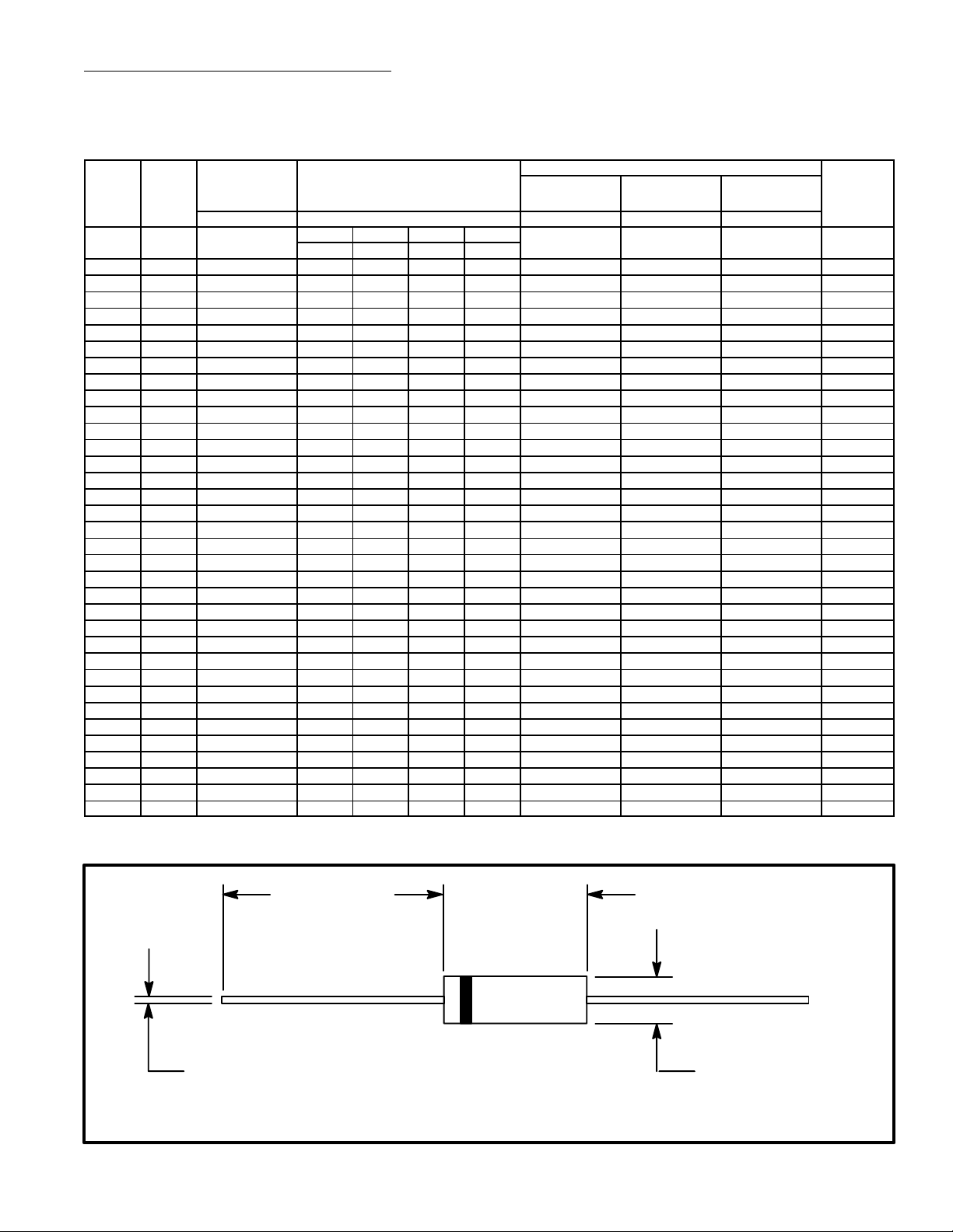
Electrical Characteristics (Cont’d):
Clamping Factor: 1.33 @ full rated power
1.20 @ 50% rated power
The clamping factor is defined as: The ratio of the actual V
(Clamping voltage) to the actual BV
C
(Breakdown Voltage) as measured on a specific device.
Maximum Ratings
NTE Type
Number
Diagram
Number
Maximum Reverse
Stand Off Voltage
(Volts)
V
R
Breakdown Voltage @ I
(Volts)
V
Min Typ Max IT mA
BR
T
Clamping Voltage
(1msec)
@ I
pp
(Volts)
V
C
Reverse Leakage
Current @ V
(µA)
I
R
R
Peak Pulse
Current
(Amps)
I
pp
Temperature
Coefficient
of BV%/°C
4920 183 12.80 14.30 15.00 15.80 1.0 21.2 5.0 71.00 0.084
4922 183 13.60 15.20 16.00 16.80 1.0 22.5 5.0 67.00 0.086
4926 183 15.30 17.10 18.00 18.90 1.0 25.2 5.0 59.50 0.088
4928 183 17.10 19.00 20.00 21.00 1.0 27.7 5.0 54.00 0.090
4932 183 20.50 22.80 24.00 25.20 1.0 33.2 5.0 45.00 0.094
4934 183 23.10 25.70 27.05 28.40 1.0 37.5 5.0 40.00 0.096
4936 183 25.60 28.50 30.00 31.50 1.0 41.4 5.0 36.00 0.097
4938 183 28.20 31.40 33.00 34.70 1.0 45.7 5.0 33.00 0.098
4940 183 30.80 34.20 36.00 37.80 1.0 49.9 5.0 30.00 0.099
4942 183 33.30 37.10 39.00 41.00 1.0 53.9 5.0 28.00 0.100
4944 183 36.80 40.90 43.00 45.20 1.0 59.3 5.0 25.30 0.101
4946 183 40.20 44.70 47.00 49.40 1.0 64.8 5.0 23.20 0.101
4950 183 43.60 48.50 51.05 53.60 1.0 70.1 5.0 21.40 0.102
4952 183 47.80 53.20 56.00 58.80 1.0 77.0 5.0 19.50 0.103
4954 183 53.00 58.90 62.00 65.10 1.0 85.0 5.0 17.70 0.104
4958 183 58.10 64.60 68.00 71.40 1.0 92.0 5.0 16.30 0.104
4960 183 64.10 71.30 75.00 78.80 1.0 103.0 5.0 14.60 0.105
4962 183 70.10 77.90 82.00 86.10 1.0 113.0 5.0 13.30 0.105
4964 183 77.80 86.50 91.00 95.50 1.0 125.0 5.0 12.00 0.106
4966 183 85.50 95.00 100.00 105.00 1.0 137.0 5.0 11.00 0.106
4968 183 94.00 105.00 110.00 116.00 1.0 152.0 5.0 9.90 0.107
4970 183 102.00 114.00 120.00 126.00 1.0 165.0 5.0 9.10 0.107
4972 183 111.00 124.00 130.00 137.00 1.0 179.0 5.0 8.40 0.107
4974 183 121.00 135.00 150.00 165.00 1.0 215.0 5.0 7.00 0.108
4976 183 136.00 152.00 160.00 168.00 1.0 219.0 5.0 6.80 0.108
4978 183 145.00 162.00 170.00 179.00 1.0 234.0 5.0 6.40 0.108
4980 183 154.00 171.00 180.00 189.00 1.0 246.0 5.0 6.10 0.108
4982 183 185.00 209.00 220.00 231.00 1.0 328.0 5.0 4.60 0.109
4984 183 214.00 237.00 250.00 263.00 1.0 344.0 5.0 5.00 0.109
4988 183 171.00 190.00 200.00 210.00 1.0 274.0 5.0 5.50 0.108
4990 183 256.00 285.00 300.00 315.00 1.0 414.0 5.0 3.58 0.110
4992 183 273.00 304.00 320.00 336.00 1.0 438.0 5.0 4.50 0.110
4994 183 300.00 333.00 350.00 368.00 1.0 482.0 5.0 3.08 0.110
4996 183 342.00 380.00 400.00 420.00 1.0 548.0 5.0 2.78 0.110
4998 183 376.00 418.00 440.00 462.00 1.0 603.0 5.0 3.50 0.110
Note 1. Normal selection of a zener transient over voltage suppressor is by rated stand–off voltage
(V
) and should be equal or greater than DC or continuous peak operating voltage.
WM
1.100
(27.94)
Min
.042 (1.07) Dia Max
.375
(9.52)
Max
.205 (5.21)
Dia Max
Color Band Denotes Cathode
 Loading...