

NTE NTE484 Datasheet
NTE484
Silicon NPN Transistor
RF Power Output for Mobile Use,
= 25W @ 947MHz
P
O
Description:
The NTE484 is a 12.5 Volt epitaxial silicon NPN planer transistor designed for primarily for 800MHz
mobile communications. This device is internally input matched in the common base configuration
for extremely broadband performance and optimum gain characteristics.
Features:
D Designed for 800 MHz Mobile Communications Equipment
D 25W Min., with Greater than 5dB Gain at 836MHz
D Withstands Infinite VSWR at Rated Operating Conditions
D Internal Input matched “Tuned Q”
D Common Base Configuration
Absolute Maximum Ratings
Collector–Base Voltage, V
Collector–Emitter Voltage, V
Emitter–Base Voltage, V
Maximum Collector Current, I
Total Device Dissipation (At +25°C), P
Operating Junction Temperature, T
Storage Temperature Range, T
: (TC = +25°C unless othrwise specified)
CBO
CEO
EBO
C
tot
J
stg
Thermal Resistance, Junction–to–Case, R
Electrical Characteristic
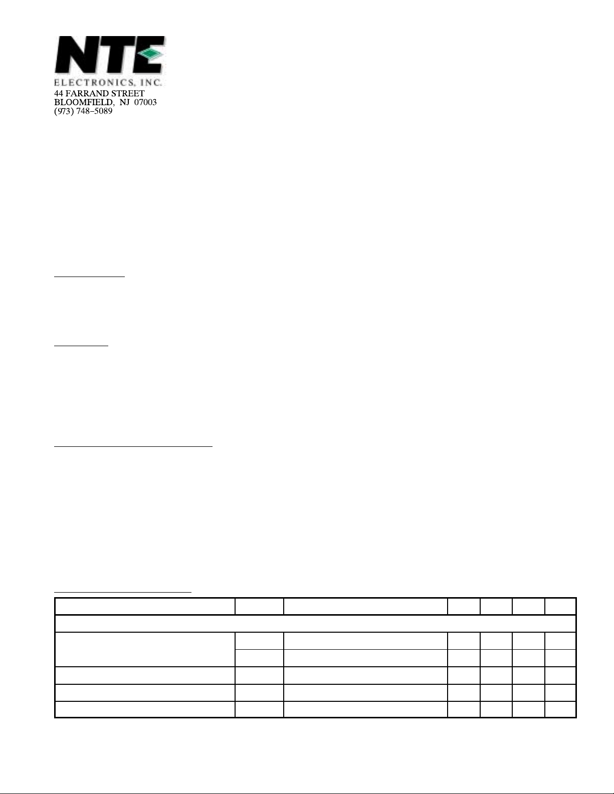
Parameter Symbol Test Conditions Min Typ Max Unit
Static
Collector–Emitter Breakdown Voltage V
Emitter–Base Breakdown Voltage V
Collector Cutoff Current I
DC Current Gain h
: (TC = +25°C unless otherwise specified)
(BR)CEOIC
V
(BR)CESIC
(BR)EBOIE
CES
FE
+200°C. . . . . . . . . . . . . . . . . . . . . . . . . . . . . . . . . . . . . . . . . . . . . . .
–65° to +150°C. . . . . . . . . . . . . . . . . . . . . . . . . . . . . . . . . . . . . . . . . .
thJC
= 50mA, IB = 0, Note 1 16 – – V
= 50mA, VBE = 0, Note 1 36 – – V
= 10mA, IC = 0 4 – – V
VCE = 15V, VBE = 0 – – 10 mA
VCE = 6V, IC = 1A 20 – –
2.3°C/W. . . . . . . . . . . . . . . . . . . . . . . . . . . . . . . . . . . . .
36V. . . . . . . . . . . . . . . . . . . . . . . . . . . . . . . . . . . . . . . . . . . . . . . . . . . . . . .
16V. . . . . . . . . . . . . . . . . . . . . . . . . . . . . . . . . . . . . . . . . . . . . . . . . . . . . .
4V. . . . . . . . . . . . . . . . . . . . . . . . . . . . . . . . . . . . . . . . . . . . . . . . . . . . . . . . . .
10A. . . . . . . . . . . . . . . . . . . . . . . . . . . . . . . . . . . . . . . . . . . . . . . . . . . . . . .
75W. . . . . . . . . . . . . . . . . . . . . . . . . . . . . . . . . . . . . . . . . . . . . .
Note 1. Pulsed through 25mH indicator.
Electrical Characteristic (Cont’d): (TC = +25°C unless otherwise specified)
Parameter Symbol Test Conditions Min Typ Max Unit
Dynamic
Output Power P
Power Gain P
Impedance Z
Output Capacitance C
VCE = 12.5V, f = 836MHz 25 – – W
O
VCE = 12.5V, f = 836MHz 5 – – dB
G
VCE = 12.5V, PO= 25W, f = 836MHz – 4.9– j5.8 – Ω
s
Z
cl
VCB = 12.5V, IE = 0, f = 1MHz – – 65 pF
ob
– 1.4– j3.5 – Ω
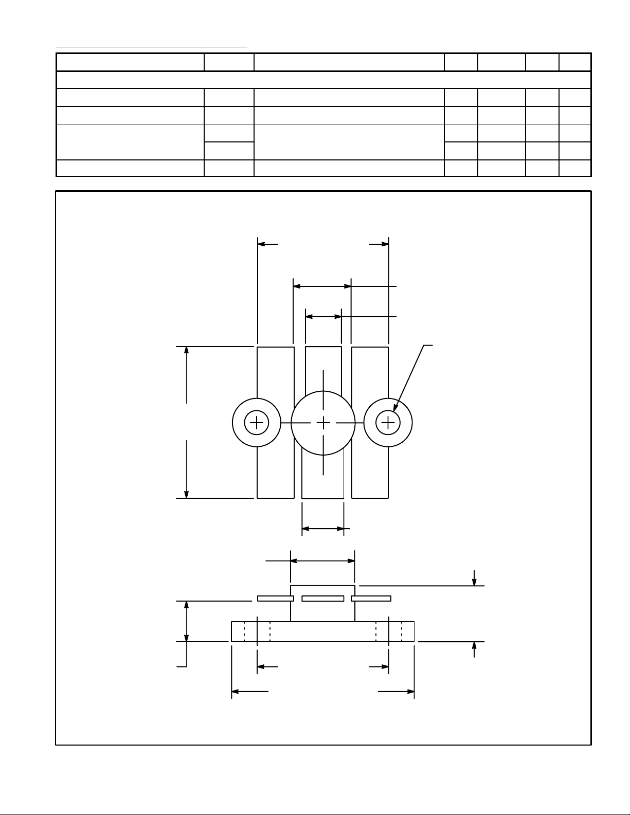
.725 (18.42)
.325 (8.28) Max
.195 (4.97) Max
.130 (3.3) Dia
BC
.960
(24.38)
Max
.380 (5.72) Dia Max
.180
(4.57)
Max
EB
.225 (5.72) Max
.285
(7.25)
Max
.730 (18.54)
.960 (24.38) Max
 Loading...