

NTE NTE477 Datasheet
NTE477
Silicon NPN Transistor
RF Power Output
Description:
The NTE477 is a silicon NPN epitaxial planar type transistor designed for RF power amplifiers in VHF
band mobile radio applications.
Features:
D High power gain: Gpe ≥ 8.2dB @ VCC = 13.5V; VO = 40W; t = 175MHz
D Emitter ballasted construction and gold metallization for high reliability, and good performances
D Low thermal resistance ceramic package with flange
D Ability of withstanding more than 20:1 load VSWR when operated at VCC = 15.2V,
P
= 40W, f = 175MHz, TC = 25°C
O
Applications:
30 to 35 watts output power amplifiers in VHF band mobile radio applications.
Absolute Maximum Ratings
Collector–Base Voltage, V
Emitter–Base Voltage, V
Collector–Emitter Voltage (R
Collector Current, I
Collector Dissipation, P
C
C
: (TC = +25°C unless otherwise specified)
CBO
EBO
= ∞), V
BE
CEO
TA = +25°C 4.5W. . . . . . . . . . . . . . . . . . . . . . . . . . . . . . . . . . . . . . . . . . . . . . . . . . . . . . . . . . . . . . . .
T
= +25°C 75W. . . . . . . . . . . . . . . . . . . . . . . . . . . . . . . . . . . . . . . . . . . . . . . . . . . . . . . . . . . . . . . .
C
Junction Temperature, T
Storage Temperature Range, T
j
stg
Thermal Resistance, Junction–to–Ambient, R
Thermal Resistance, Junction–to–Case, R
Electrical Characteristics
Parameter Symbol Test Conditions Min Typ Max Unit
Emitter–Base Breakdown Voltage V
Collector–Base Breakdown Voltage V
Collector–Emitter Breakdown Voltage V
: (TC = +25°C unless otherwise specified)
thJC
(BR)EBOIE
(BR)CBOIO
(BR)CEOIO
–55° to +175°C. . . . . . . . . . . . . . . . . . . . . . . . . . . . . . . . . . . . . . . . . .
thJA
= 10mA, IO = 0 3 – – V
= 10mA, IE = 0 35 – – V
= 0.1A, RBE = ∞ 17 – – V
33.3°C/W. . . . . . . . . . . . . . . . . . . . . . . . . . . . . . . . . .
35V. . . . . . . . . . . . . . . . . . . . . . . . . . . . . . . . . . . . . . . . . . . . . . . . . . . . . . .
4V. . . . . . . . . . . . . . . . . . . . . . . . . . . . . . . . . . . . . . . . . . . . . . . . . . . . . . . . . .
17V. . . . . . . . . . . . . . . . . . . . . . . . . . . . . . . . . . . . . . . . . . .
10A. . . . . . . . . . . . . . . . . . . . . . . . . . . . . . . . . . . . . . . . . . . . . . . . . . . . . . . . . . . . . . . .
+175°C. . . . . . . . . . . . . . . . . . . . . . . . . . . . . . . . . . . . . . . . . . . . . . . . . . . . . . . . .
2°C/W. . . . . . . . . . . . . . . . . . . . . . . . . . . . . . . . . . . . . . .
Electrical Characteristics (Cont’d): (TC = +25°C unless otherwise specified)
Parameter Symbol Test Conditions Min Typ Max Unit
Collector Cutoff Current I
Emitter Cutoff Current I
DC Forward Current Gain h
Output Power P
CBO
EBO
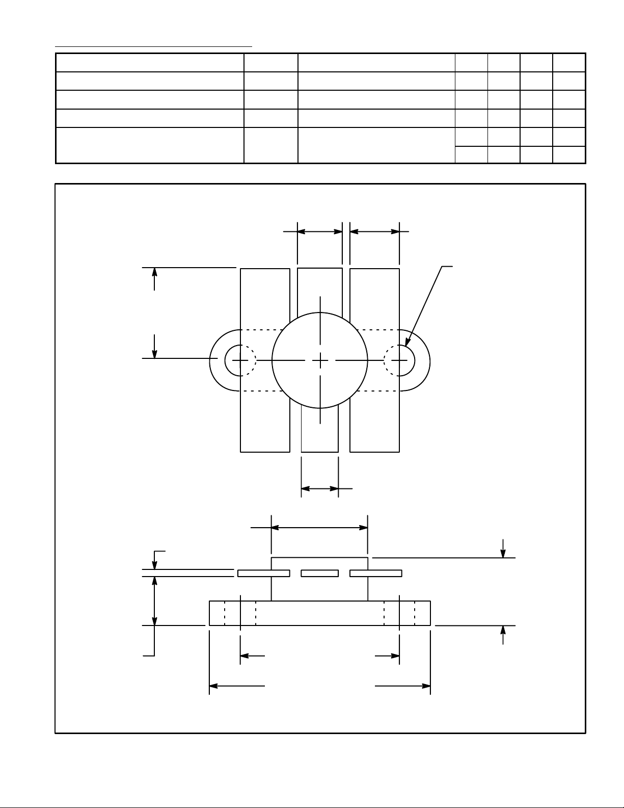
.205 (5.18)
EB
.405
(10.3)
Min
FE
VOB = 15V, IE = 0 – – 2.5 mA
VEB = 3V, IO = 0 – – 2 mA
VCE = 10V, IC = 0.2A 10 60 180 –
VCC = 13.5V Pin = 6W,
O
f = 175MHz
40 45 – W
60 70 – %
.215 (5.48)
.122 (3.1) Dia
.160
(4.06)
CE
.155 (3.94)
.500 (12.7) Dia
.005 (0.15)
.270
(6.85)
.725 (18.43)
.975 (24.78)
 Loading...