

NTE NTE389 Datasheet

NTE389
Silicon NPN Transistor
Horizontal Output
Description:
The NTE389 is a high voltage silicon NPN power transistor in a TO3 type case designed for use in
CRT horizontal deflection circuits.
Features:
D Collector–Emitter Voltage: V
D Glass Passivated Base–Collector Junction
D Forward Bias Safe Operating Area @ 50µs = 20A, 300V
D Switching Times with Inductive Loads: tf = 0.5µs (Typ) @ IC = 3A
Absolute Maximum Ratings:
Collector–Emitter Voltage, V
Collector–Emitter Voltage, V
Emitter–Base Voltage, V
CEO
CEX
EBO
Continuous Collector Current, I
Continuous Base Current, I
Continouos Emitter Current, I
Total Power Dissipation, P
B
E
D
TC = +25°C 100W. . . . . . . . . . . . . . . . . . . . . . . . . . . . . . . . . . . . . . . . . . . . . . . . . . . . . . . . . . . . . . . .
TC = +100°C 40W. . . . . . . . . . . . . . . . . . . . . . . . . . . . . . . . . . . . . . . . . . . . . . . . . . . . . . . . . . . . . . . .
Derate Above +25°C 0.8W/°C. . . . . . . . . . . . . . . . . . . . . . . . . . . . . . . . . . . . . . . . . . . . . . . . . . . . . .
CEX
C
= 1500V
750V. . . . . . . . . . . . . . . . . . . . . . . . . . . . . . . . . . . . . . . . . . . . . . . . . . . . .
1500V. . . . . . . . . . . . . . . . . . . . . . . . . . . . . . . . . . . . . . . . . . . . . . . . . . . .
5V. . . . . . . . . . . . . . . . . . . . . . . . . . . . . . . . . . . . . . . . . . . . . . . . . . . . . . . . . .
4A. . . . . . . . . . . . . . . . . . . . . . . . . . . . . . . . . . . . . . . . . . . . . . . . . . . . . .
3A. . . . . . . . . . . . . . . . . . . . . . . . . . . . . . . . . . . . . . . . . . . . . . . . . . . . . . . . . .
7A. . . . . . . . . . . . . . . . . . . . . . . . . . . . . . . . . . . . . . . . . . . . . . . . . . . . . . . .
Operating Junction Temperature Range, T
Storage Temperature Range, T
stg
Thermal Resistance, Junction–to–Case, R
J
thJC
Maximum Lead Temperature (For Soldering, 1/8” from Case for 5sec), T
–65° to +150°C. . . . . . . . . . . . . . . . . . . . . . . . . . . . . . . . . .
–65° to +150°C. . . . . . . . . . . . . . . . . . . . . . . . . . . . . . . . . . . . . . . . . .
1.25°C/W. . . . . . . . . . . . . . . . . . . . . . . . . . . . . . . . . . . .
L
+275°C. . . . . . . . . . . . . .
Electrical Characteristics: (TC = +25°C unless otherwise specified)
Parameter Symbol Test Conditions Min Typ Max Unit
OFF Characteristics (Note 1)
Collector–Emitter Sustaining Voltage V
Collector Cutoff Current I
Emitter Cutoff Current I
ON Characteristics (Note 1)
Collector–Emitter Saturation Voltage V
Base–Emitter Saturation Voltage V
Dynamic Characteristics
Current Gain – Bandwidth Product f
Output Capacitance C
Switching Characteristics
Fall Time t
CEO(sus)IC
CE(sat)IC
BE(sat)IC
CES
EBO
T
ob
f
= 50mA, IB = 0 750 – – V
VCE = 1500V, VBE = 0 – – 1.0 mA
VBE = 5V, IC = 0 – – 1.0 mA
= 3A, IB = 1.2A – – 5.0 V
= 3A, IB = 1.2A – – 1.5 V
IC = 0.1A, VCE = 5V, f
VCB = 10V, IE = 0, f = 0.1MHz – 90 – pF
IC = 3A, IB1 = 1.2A, LB = 8µH – 0.5 1.0 µs
Note 1. Pulse Test: Pulse Width ≤ 300µs, Duty Cycle = 2%.
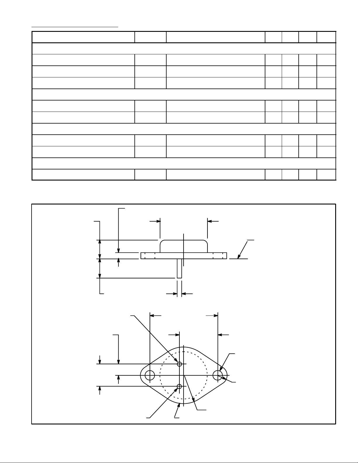
.135 (3.45) Max
.350 (8.89)
.875 (22.2)
Dia Max
= 1MHz – 4 – MHz
test
.215 (5.45)
.430
(10.92)
Emitter
Seating
Plane
.040 (1.02).312 (7.93) Min
1.187 (30.16)
.665
(16.9)
.156 (3.96) Dia
(2 Holes)
.188 (4.8) R Max
.525 (13.35) R Max
Collector/CaseBase
 Loading...