

NTE NTE368 Datasheet
NTE368
Silicon NPN Transistor
RF Power Output
PO = 60W @ 512MHz
Description:
The NTE368 is a silicon NPN transistor designed for 12.5 Volt UHF large–signal amplifier applications
in industrial and commercial FM equipment operating to 512MHz.
Features:
D Specified 12.5 Volt, 470MHz Characteristic:
Output Power = 60 Watts
Minimum Gain = 4.4dB
Efficiency = 55%
D Characterized with Series Equivalent Large–Signal Impedance Parameters
D Built–In Matching Network for Broadband Operation
D Tested for Load Mismatch Stress at all Phase Angles with 20:1 VSWR @ 16–volt High Line
and Overdrive
Absolute Maximum Ratings:
Collector–Emitter Voltage, V
Collector–Base Voltage, V
Emitter–Base Voltage, V
Collector Current–Continuous, I
Total Device Dissipation (TC = +25°C), P
CEO
CBO
EBO
C
D
Derate above 25°C 1.0W/°C. . . . . . . . . . . . . . . . . . . . . . . . . . . . . . . . . . . . . . . . . . . . . . . . . . . . . . .
Storage Temperature Range, T
Thermal Resistance, Junction–to–Case, R
–65° to +150°C. . . . . . . . . . . . . . . . . . . . . . . . . . . . . . . . . . . . . . . . . .
stg
thJC
Electrical Characteristics: (TC = +25°C unless otherwise specified)
Parameter Symbol Test Conditions Min Typ Max Unit
OFF Characteristics
Collector–Emitter Breakdown Voltage V
V
Emitter–Base Breakdown Voltage V
Collector Cutoff Current I
(BR)CEOIC
(BR)CESIC
(BR)EBOIE
CES
= 50mA, IB = 0 16 – – V
= 50mA, VBE = 0 36 – – V
= 5mA, IC = 0 4 – – V
VCE = 15V, VBE = 0, TC = +25°C – – 15 mA
16V. . . . . . . . . . . . . . . . . . . . . . . . . . . . . . . . . . . . . . . . . . . . . . . . . . . . . .
36V. . . . . . . . . . . . . . . . . . . . . . . . . . . . . . . . . . . . . . . . . . . . . . . . . . . . . . .
4V. . . . . . . . . . . . . . . . . . . . . . . . . . . . . . . . . . . . . . . . . . . . . . . . . . . . . . . . . .
11A. . . . . . . . . . . . . . . . . . . . . . . . . . . . . . . . . . . . . . . . . . . . . . . . . . . . .
175W. . . . . . . . . . . . . . . . . . . . . . . . . . . . . . . . . . . . . . . . . . .
1.0°C/W. . . . . . . . . . . . . . . . . . . . . . . . . . . . . . . . . . . . .
Electrical Characteristics (Cont’d): (TC = +25°C unless otherwise specified)
Parameter Symbol Test Conditions Min Typ Max Unit
ON Characteristics
DC Current Gain h
FE
VCE = 5V, IC = 6A 20 70 150
Dynamic Characteristics
Output Capacitance C
VCB = 12.5V, IE = 0, f = 1MHz – 130 150 pF
ob
Functional Test
Common–Emitter Amplifier Power Gain G
Input Power P
PE
in
P
= 60W, VCC = 12.5V, f = 470MHz
OUT
4.4 5.0 – dB
– 19 22 W
Collector Efficiency η 55 60 – %
Output Mismatch Stress ψ VCC = 16V, Pin = 26W, f = 470MHz,
VSWR = 20:1, All Phase Angles
No Degradation in
Output Power
Note 1. y = Mismatch stress factor – the electrical criterion established to verify the device resistance
to load mismatch failure. The mismatch stress test is accomplished in a standard test fixture
terminated in a 20:1 minimum load mismatch at all phase angles.
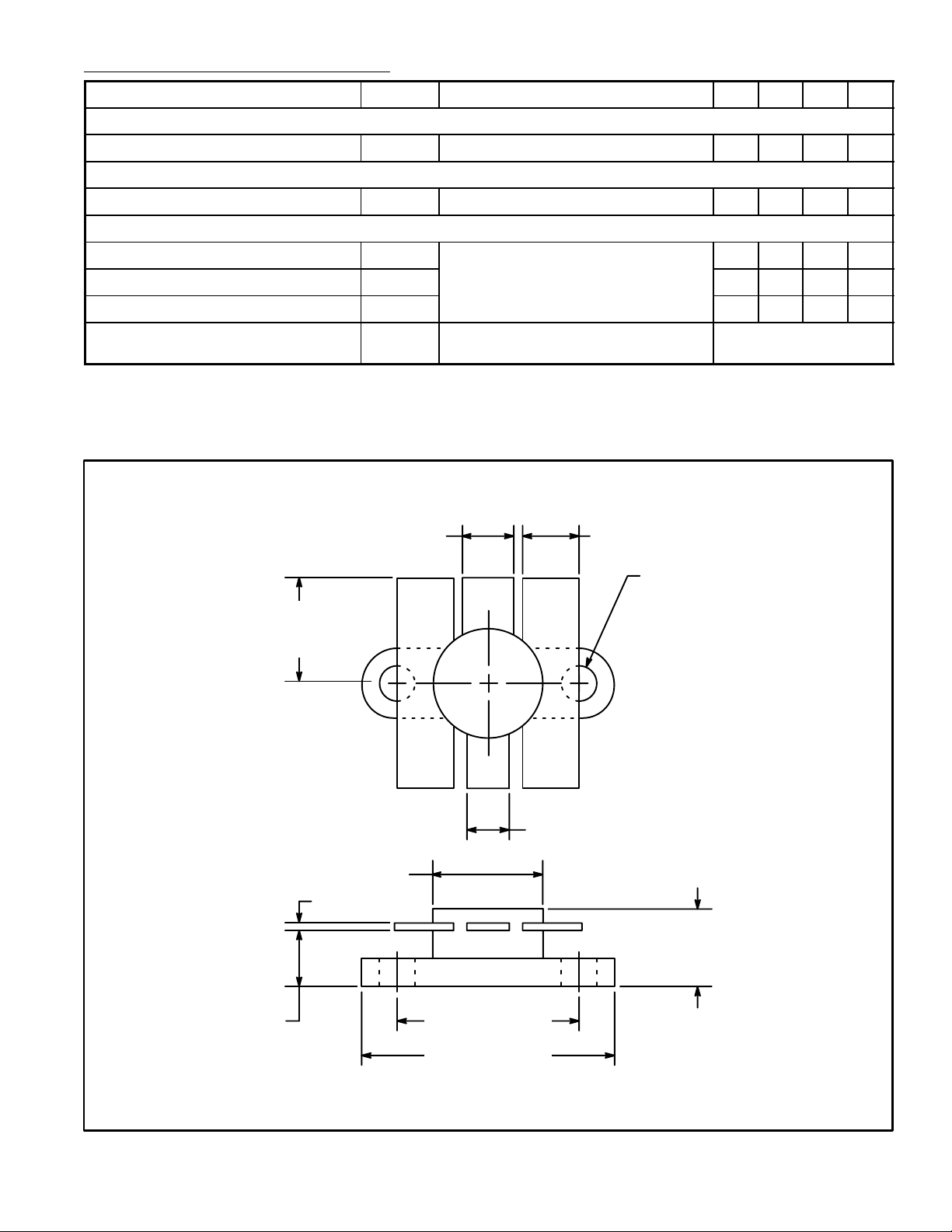
.205 (5.18)
EB
.405
(10.3)
Min
.215 (5.48)
.122 (3.1) Dia
.160 (4.06)
CE
.155 (3.94)
.500 (12.7) Dia
.005 (0.15)
.270
(6.85)
.725 (18.43)
.975 (24.78)
 Loading...