

NTE NTE363 Datasheet
NTE363
Silicon NPN Transistor
RF Power Amp, PO = 4W
Description:
The NTE363 is a 12.5V epitaxial silicon NPN planer transistor designed primarily for UHF communications.
Features:
D Designed for UHF Military and Commercial Equipment
D 4W (Min) with Greater than 8dB Gain
D Withstands Infinite VSWR Under Operating Conditions
D Low Inductance Stripline Package
D Emitter Stabilized
Absolute Maximum Ratings:
Collector–Base Voltage, V
Collector–Emitter Voltage, V
Emitter–Base Voltage, V
Maximum Collector Current, I
Total Device Dissipation (TC = +25°C), P
Operating Junction Temperature, T
Storage Temperature Range, T
CBO
CEO
EBO
C
T
J
stg
Thermal Resistance, Junction–to–Case, R
–65° to +200°C. . . . . . . . . . . . . . . . . . . . . . . . . . . . . . . . . . . . . . . . . .
thJC
36V. . . . . . . . . . . . . . . . . . . . . . . . . . . . . . . . . . . . . . . . . . . . . . . . . . . . . . .
16V. . . . . . . . . . . . . . . . . . . . . . . . . . . . . . . . . . . . . . . . . . . . . . . . . . . . . .
4V. . . . . . . . . . . . . . . . . . . . . . . . . . . . . . . . . . . . . . . . . . . . . . . . . . . . . . . . . .
800mA. . . . . . . . . . . . . . . . . . . . . . . . . . . . . . . . . . . . . . . . . . . . . . . . . . . .
15W. . . . . . . . . . . . . . . . . . . . . . . . . . . . . . . . . . . . . . . . . . . .
+200°C. . . . . . . . . . . . . . . . . . . . . . . . . . . . . . . . . . . . . . . . . . . . . . .
11.6°C/W. . . . . . . . . . . . . . . . . . . . . . . . . . . . . . . . . . . .
Electrical Characteristics:
Parameter Symbol Test Conditions Min Typ Max Unit
Collector–Emiter Breakdown Voltage V
Emitter–Base Breakdown Voltage V
Collector Cutoff Current I
DC Current Gain h
(BR)CEOIC
V
(BR)CESIC
(BR)EBOIE
CBO
FE
Note 1. Pulsed throught 25MH inductor.
= 100mA, IB = 0, Note 1 16 – – V
= 100mA, IBE = 0, Note 1 36 – – V
= 2mA, IC = 0 4 – – V
VCB = 5V, IE = 0 – – 1.0 mA
VCE = 5V, IC = 200mA 20 – –
Electrical Characteristics (Cont’d):
Parameter Symbol Test Conditions Min Typ Max Unit
RF Characteristics, Small–Signal
Output Capacitance C
Input Capacitance C
RF Characteristics, Large–Signal
Amplifier Power Out P
Amplifier Power Gain P
Input Impedance Z
Output Impedance Z
E
ob
ib
O
g
in
out
VCB = 12.5V, IC = 0 – – 25 pF
VEB = 500mV, IC = 0 – 60 – pF
470MHz/12.5V 4 – – W
8 – – dB
2.0 + J.96 Ω
6.0 – J3.4 Ω
B
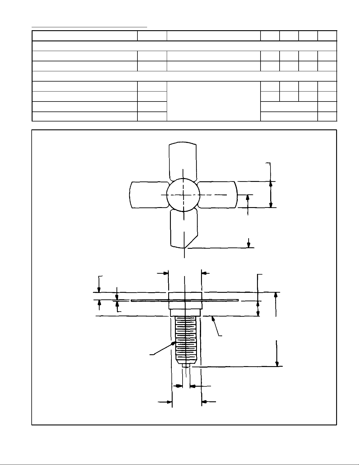
.225 (5.72)
E
.530
(13.46)
C
.063 (1.62)
.005 (0.15)
8–32 NC–3A
.282 (7.17)
Dia
Seating
Plane
Wrench Flat
.250 (6.35) Dia
.123 (3.12)
.630
(16.0)
 Loading...