

NTE NTE355 Datasheet
NTE355
Silicon NPN Transistor
RF Power Output
PO = 30W @ 175MHz
Description:
The NTE355 is designed for 12.5 Volt VHF large–signal amplifier applications required in military and
industrial equipment operating to 250MHz.
Features:
D Balanced Emitter Construction with Isothermal Resistor Design to Provide the Designer with
the Optimum in Transistor Ruggedness.
D Low lead Inductance Stripline Packaging for Easier Design and Increased Broadband Capabilities
D Flange Package for Easy Mounting and Better Thermal Conductivity to Heat Sink.
D Exceptional Power Output Stability versus Temperature.
Absolute Maximum Ratings:
Collector–Emitter Voltage, V
Collector–Base Voltage, V
Emitter–Base Voltage, V
Collector Current–Continuous, I
Total Device Dissipation (TC = +25°C, Note 1), P
CEO
CBO
EBO
C
D
Derate Above 25°C 228mW/°C. . . . . . . . . . . . . . . . . . . . . . . . . . . . . . . . . . . . . . . . . . . . . . . . . . . . .
Storage Temperature Range, T
stg
–65° to +200°C. . . . . . . . . . . . . . . . . . . . . . . . . . . . . . . . . . . . . . . . . .
18V. . . . . . . . . . . . . . . . . . . . . . . . . . . . . . . . . . . . . . . . . . . . . . . . . . . . . .
36V. . . . . . . . . . . . . . . . . . . . . . . . . . . . . . . . . . . . . . . . . . . . . . . . . . . . . . .
4V. . . . . . . . . . . . . . . . . . . . . . . . . . . . . . . . . . . . . . . . . . . . . . . . . . . . . . . . . .
4A. . . . . . . . . . . . . . . . . . . . . . . . . . . . . . . . . . . . . . . . . . . . . . . . . . . . . .
40W. . . . . . . . . . . . . . . . . . . . . . . . . . . . . . . . . . . . .
Note 1. This device is designed for RF operation. The total device dissipation rating applies only
when the device is operated as an RF amplifier.
Electrical Characteristics: (TC = +25°C unless otherwise specified)
Parameter Symbol Test Conditions Min Typ Max Unit
OFF Characteristics
Collector–Emitter Breakdown Voltage V
V
Emitter–Base Breakdown Voltage V
Collector Cutoff Current I
(BR)CEOIC
(BR)CESIC
(BR)EBOIE
CBO
I
CES
= 50mA, IB = 0 18 – – V
= 15mA, VBE = 0 36 – – V
= 5mA, IC = 0 4 – – V
VCB = 15V, IE = 0 – – 1.0 mA
VCE = 15V, VBE = 0, TC = +55°C – – 10 mA
Electrical Characteristics (Cont’d): (TC = +25°C unless otherwise specified)
Parameter Symbol Test Conditions Min Typ Max Unit
ON Characteristics
DC Current Gain h
Dynamic Characteristics
Output Capacitance C
Functional Test
Common–Emitter Amplifier Power Gain G
Collector Efficiency η P
FE
ob
PE
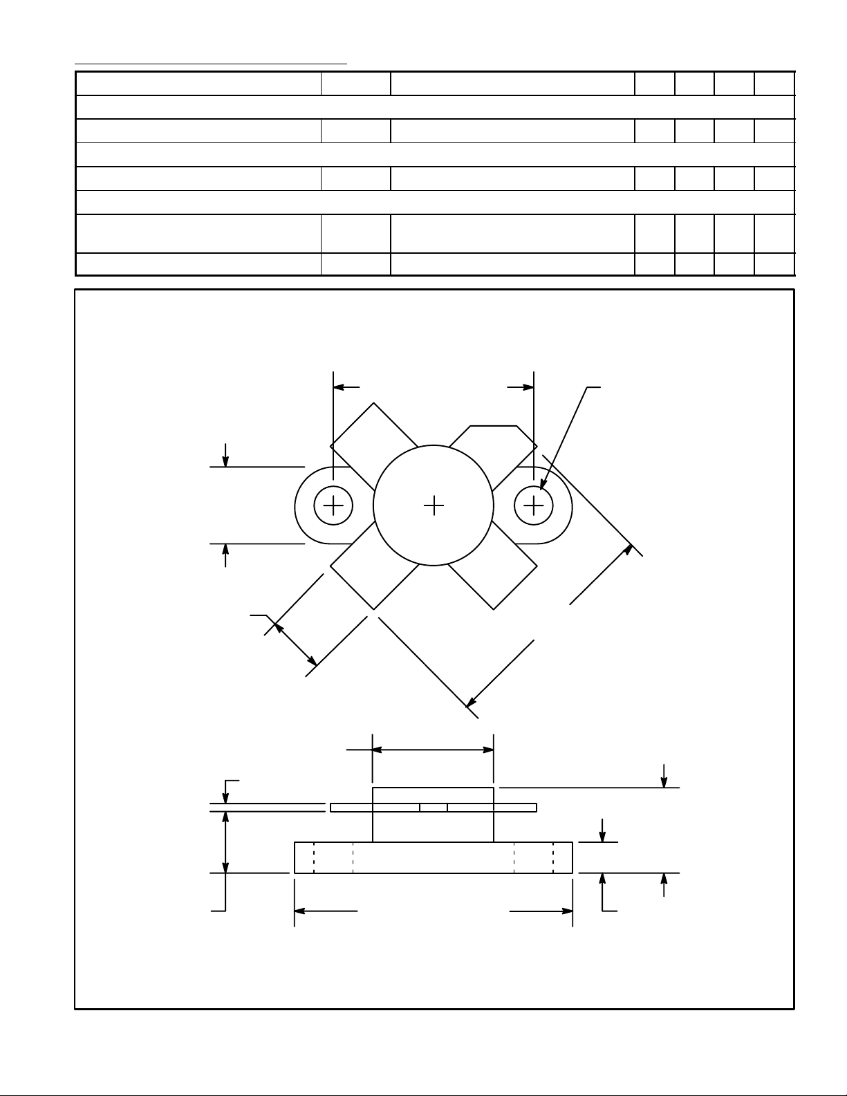
.725 (18.42)
EC
.250
(6.35)
VCE = 5V, IC = 500mA 15 – –
VCB = 12.5V, IE = 0, f = 100kHz – 150 190 pF
P
= 30W, VCC = 12.5V,
OUT
ICmax = 3.4A, f = 175MHz
= 30W, VCC = 12.5V, f = 175MHz 60 – – %
OUT
5.7 – – dB
.122 (3.1) Dia
(2 Holes)
.225 (5.72)
.185 (4.7)
.378 (9.56)
.005 (0.15)
BE
.860 (21.84)
.975 (24.77)
.255
(6.5)
.085 (2.14)
 Loading...