

NTE NTE3311 Datasheet
NTE3311
Insulated Gate Bipolar Transistor
N–Channel Enhancement Mode,
High Speed Switch
Features:
D High Input Impedance
D High Speed
D Low Saturation Voltage
D Enhancement Mode
Applications:
D High Power Switching
D Motor Control
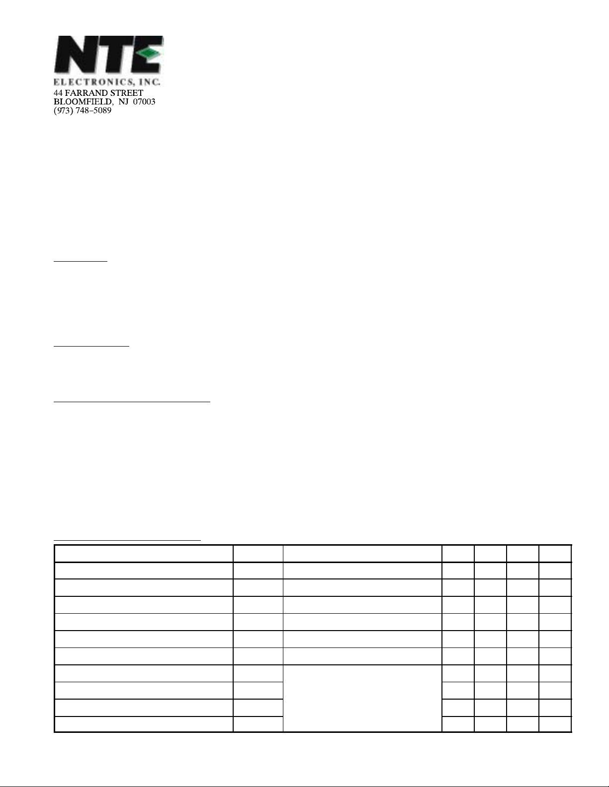
Absolute Maximum Raings: (TA = +25°C unless otherwise specified)
Collector–Emitter Voltage, V
Gate–Emitter Voltage, V
Collector Current, I
C
DC 25A. . . . . . . . . . . . . . . . . . . . . . . . . . . . . . . . . . . . . . . . . . . . . . . . . . . . . . . . . . . . . . . . . . . . . . . . .
Pulse (1ms) 50A. . . . . . . . . . . . . . . . . . . . . . . . . . . . . . . . . . . . . . . . . . . . . . . . . . . . . . . . . . . . . . . . .
Collector Power Dissipation (TC = +25°C), P
Operating Junction Temperature, T
Storage Temperature Range, T
CES
GES
C
J
stg
600V. . . . . . . . . . . . . . . . . . . . . . . . . . . . . . . . . . . . . . . . . . . . . . . . . . . . .
±20V. . . . . . . . . . . . . . . . . . . . . . . . . . . . . . . . . . . . . . . . . . . . . . . . . . . . . . . .
150W. . . . . . . . . . . . . . . . . . . . . . . . . . . . . . . . . . . . . . . .
+150°C. . . . . . . . . . . . . . . . . . . . . . . . . . . . . . . . . . . . . . . . . . . . . . .
–55° to +150°C. . . . . . . . . . . . . . . . . . . . . . . . . . . . . . . . . . . . . . . . . .
Electrical Characteristics: (TA = +25°C unless otherwise specified)
Parameter Symbol Test Conditions Min Typ Max Unit
Gate Leakage Current I
Collector Cutoff Current I
Collector–Emitter Breakdown Voltage V
Gate–Emitter Cutoff Voltage V
Collector–Emitter Saturation Voltage V
Input Capacitance C
Rise Time t
Turn–On Time t
Fall Time t
Turn–Off Time t
(BR)CESIC
GE(off)IC
CE(sat)IC
GES
CES
ies
on
off
VGE = ±20V, VCE = 0 – – ±500 nA
VCE = 600V, VGE = 0 – – 1.0 mA
= 2mA, VGE = 0 600 – – V
= 25mA, VCE = 5V 3.0 – 6.0 V
= 25A, VGE = 15V – 3.0 4.0 V
VCE = 10V, VGE = 0, f = 1MHz – 1400 – pF
VCC = 300V
r
f
– 0.30 0.60 µs
– 0.40 0.80 µs
– 0.15 0.35 µs
– 0.50 1.00 µs
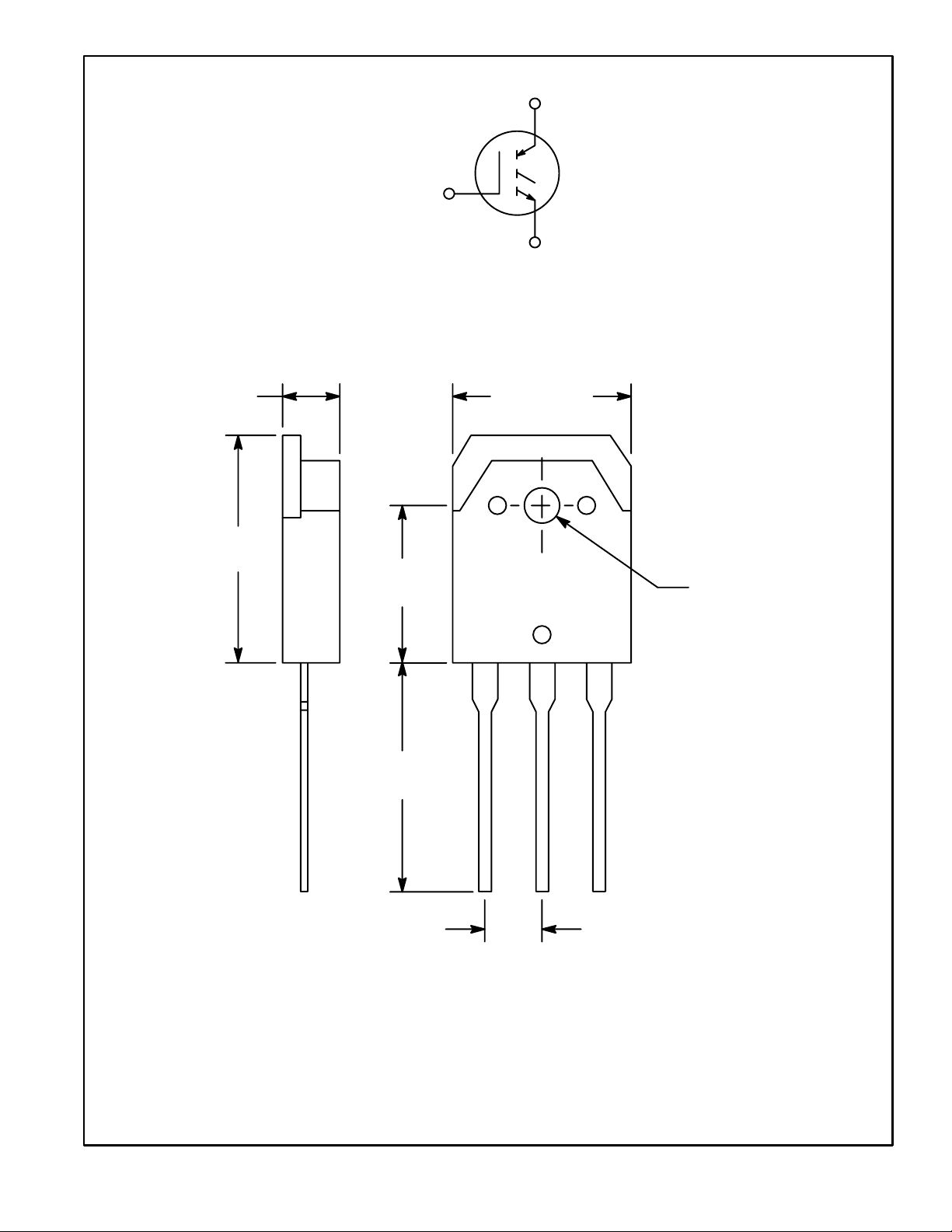
.787
(20.0)
.591
(15.02)
C
G
E
.615 (15.62).190 (4.82)
.126 (3.22) Dia
.787
(20.0)
GC/
Case
E
.215 (5.47)
 Loading...