

NTE NTE329 Datasheet

NTE329
Silicon NPN Transistor
RF Power Amp, CB
Description:
The NTE329 is designed primarily for use in large–signal output amplifier stages. Intended for use
in Citizen–Band communications equipment operating to 30MHz. High breakdown voltages allow a
high percentage of up–modulation in AM circuits.
Features:
D Specified 12.5V, 28MHz Characteristic:
Power Output = 3.5W
Power Gain = 10dB
Efficiency = 70% Typical
Absolute Maximum Ratings:
Collector–Emitter Voltage, V
Collector–Base Voltage, V
Emitter–Base Voltage, V
CEO
CBO
EBO
Continuous Collector Current, I
Total Device Dissipation (T
= +25°C, Note 1), P
C
C
D
30V. . . . . . . . . . . . . . . . . . . . . . . . . . . . . . . . . . . . . . . . . . . . . . . . . . . . . .
60V. . . . . . . . . . . . . . . . . . . . . . . . . . . . . . . . . . . . . . . . . . . . . . . . . . . . . . .
3V. . . . . . . . . . . . . . . . . . . . . . . . . . . . . . . . . . . . . . . . . . . . . . . . . . . . . . . . . .
1A. . . . . . . . . . . . . . . . . . . . . . . . . . . . . . . . . . . . . . . . . . . . . . . . . . . . . .
5W. . . . . . . . . . . . . . . . . . . . . . . . . . . . . . . . . . . . . .
Derate above 25°C 28.6mW/°C. . . . . . . . . . . . . . . . . . . . . . . . . . . . . . . . . . . . . . . . . . . . . . . . . . . .
Storage Temperature Range, T
stg
–65° to +200°C. . . . . . . . . . . . . . . . . . . . . . . . . . . . . . . . . . . . . . . . . .
Note 1. This device is designed for RF operation. The total device dissipation rating applies only
when the device is operated as an RF amplifier.
Electrical Characteristics:
Parameter Symbol Test Conditions Min Typ Max Unit
OFF Characteristics
Collector–Emitter Breakdown Voltage V
Emitter–Base Breakdown Voltage V
Collector Cutoff Current I
ON Characteristics
(TA = +25°C, unless otherwise specified)
(BR)CEOIC
V
(BR)CESIC
(BR)EBOIE
CBO
= 50mA, I
= 200mA, V
= 1mA, IC = 0 3 – – V
VCB = 15V, IE = 0 – – 0.01 mA
= 0 30 – – V
B
= 0 60 – – V
BE
DC Current Gain h
Dynamic Characteristics
Output Capacitance C
VCE = 2V, IC = 400mA 10 – – –
FE
VCB = 12.5V, IE = 0, f = 1MHz – 35 70 pF
ob
Electrical Characteristics (Cont’d): (TA = +25°C, unless otherwise specified)
Parameter Symbol Test Conditions Min Typ Max Unit
Functional Test
Common–Emitter Amplifier Power Gain G
Collector Efficiency η P
PE
P
= 3.5W, VCC = 12.5V, f = 27MHz 10 – – dB
OUT
= 3.5W, VCC = 12.5V, f = 27MHz,
OUT
62.5 70.0 – %
Note 3
Percent Up–Modulation – f = 27MHz, Note 2 – 85 – %
Parallel Equivalent Input Resistance R
Parallel Equivalent Input Capacitance C
Parallel Equivalent Output Capaciatnce C
Note 2. η = RF P
OUT
(V
100
CC
) (IC)
in
in
out
P
= 3.5W, VCC = 12.5V, f = 27MHz – 21 –
OUT
P
= 3.5W, VCC = 12.5V, f = 27MHz – 900 – pF
OUT
P
= 3.5W, VCC = 12.5V, f = 27MHz – 200 – pF
OUT
Ω
Note 3. Percentage Up–Modulation is measured by setting the Carrier Power (PC) to 3.5 Watts with
V
= 12.5Vdc and noting the power input. The peak envelope power (PEP) is noted after
CC
doubling the original power input to simulate driver modulation (at a 25% duty cycle for thermal considerations) and raising the V
to 25Vdc (to simulate the modulating voltage). Per-
CC
centage Up–Modulation is then determined by the relation:
Percentage Up–Modulation = (PEP) 1/2–1 100
P
C
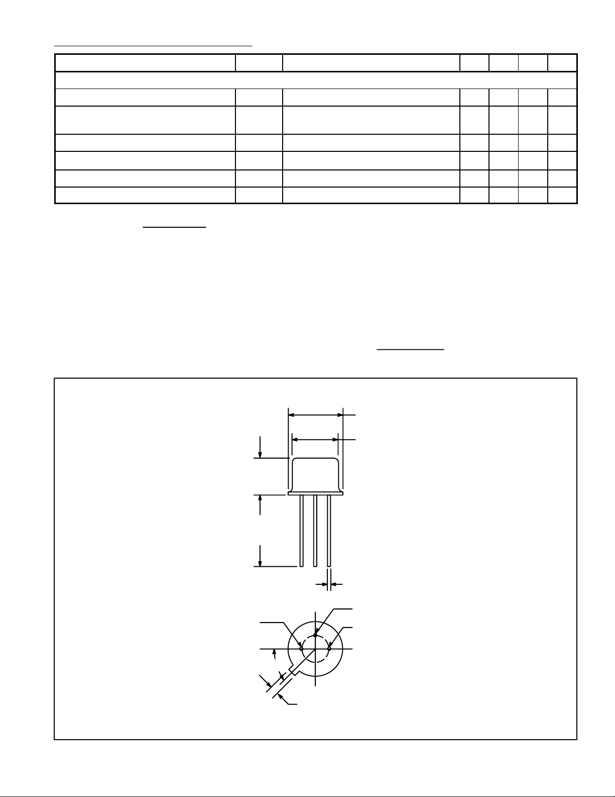
Emitter
.370 (9.39) Dia Max
.355 (9.03) Dia Max
.260
(6.6)
Max
.500
(12.7)
Min
.018 (0.45)
Base
Collector/Case
45°
.031 (.793)
 Loading...