

NTE NTE314 Datasheet
NTE314
Silicon Controlled Rectifier (SCR)
Power Regulator Switch
Description:
The NTE314 is a silicon controlled rectifier (SCR) in a TO3 type package designed for 12.5 Ampere
RMS, 400 Volt power supply and computer control applications to +100°C maximum junction.
Features:
D Low Forward “ON” Voltage
D All Diffused Junctions for Greater Parameter Uniformity
D Glass Passivated for Greater Stability
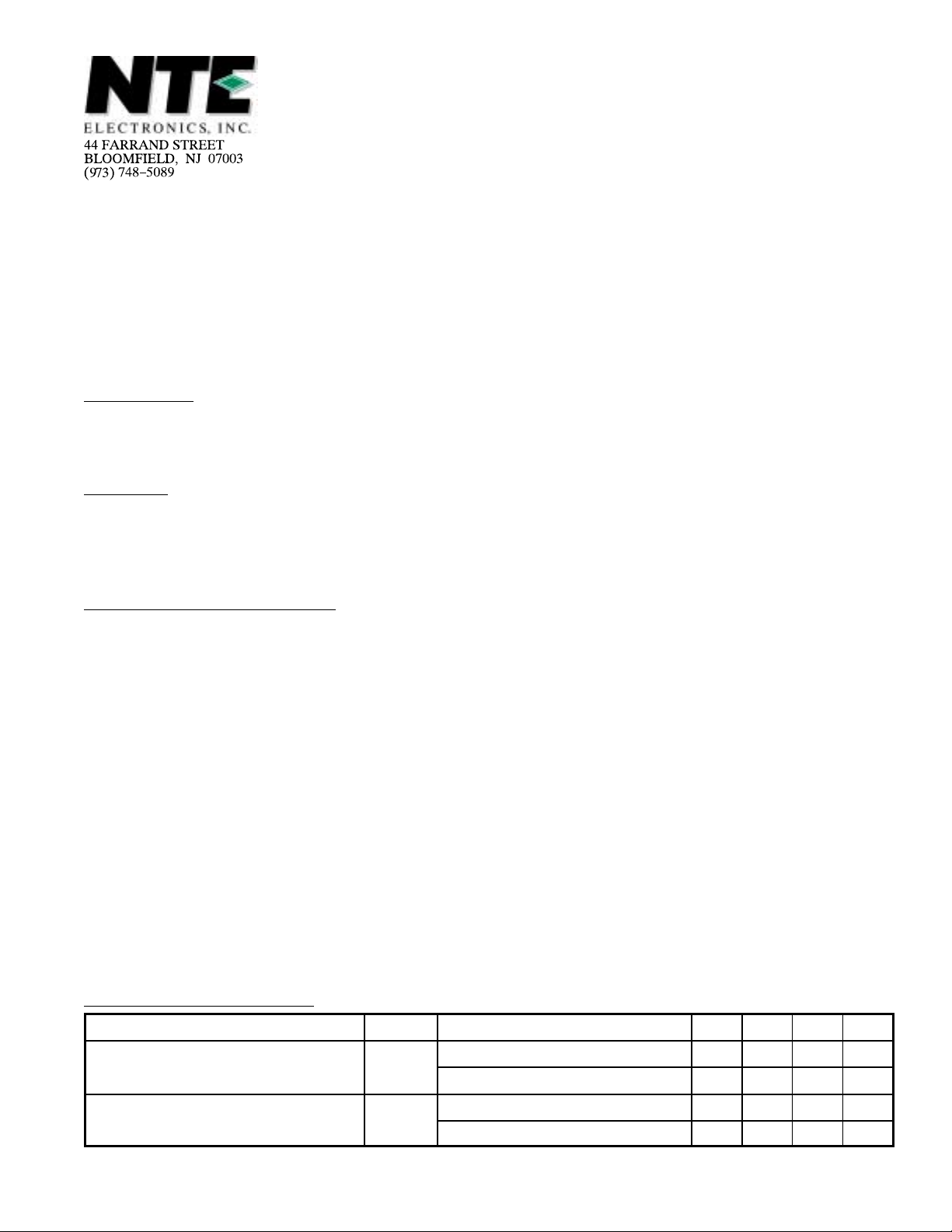
Absolute Maximum Ratings:
Peak Repetitive Forward and Reverse Blocking Voltage (Note 1), V
RMS Forward Current (T
Peak Forward Surge Current (1/2 Cycle Sine Wave, 60Hz, T
Fusing Current (T
= –40° to +100°C, t = 1 to 8.3ms), I2t 170A2s. . . . . . . . . . . . . . . . . . . . . . . . . . . . .
J
Forward Peak Gate Power, P
Forward Average Gate Power, P
Forward Peak Gate Current, I
Peak Forward Gate Voltage, V
Peak Reverse Gate Voltage, V
Operating Junction Temperature Range, T
Storage Temperature Range, T
Thermal Resistance, Junction–to–Case, R
= +80°C, All Conduction Angles), I
C
GM
G(AV)
GM
GF
GR
J
stg
thJC
T(RMS)
= –40° to +100°C), I
J
DRM
, V
RRM
TSM
–40° to +100°C. . . . . . . . . . . . . . . . . . . . . . . . . . . . . . . . . .
–40° to +125°C. . . . . . . . . . . . . . . . . . . . . . . . . . . . . . . . . . . . . . . . . .
400V. . . . . . . . . . . .
12.5A. . . . . . . . . . . . . . . . . . . .
200A. . . . .
5W. . . . . . . . . . . . . . . . . . . . . . . . . . . . . . . . . . . . . . . . . . . . . . . . . . . . . .
0.5W. . . . . . . . . . . . . . . . . . . . . . . . . . . . . . . . . . . . . . . . . . . . . . . .
2A. . . . . . . . . . . . . . . . . . . . . . . . . . . . . . . . . . . . . . . . . . . . . . . . . . . . . .
19V. . . . . . . . . . . . . . . . . . . . . . . . . . . . . . . . . . . . . . . . . . . . . . . . . . . . .
5V. . . . . . . . . . . . . . . . . . . . . . . . . . . . . . . . . . . . . . . . . . . . . . . . . . . . .
1.7°C/W. . . . . . . . . . . . . . . . . . . . . . . . . . . . . . . . . . . . .
Note 1. V
DRM
and V
can b e applied on a c ontinuous D C b asis without incurrent d amage. Ratings
RRM
apply for zero or negative gate voltage. Devices should not be tested for blocking capability
in a manner such that the voltage supplied exceeds the rated blocking voltage.
Electrical Characteristics:
Parameter Symbol Test Conditions Min Typ Max Unit
Peak Forward Blocking Current I
Peak Reverse Blocking Current I
(VD = 400V, TC = +25°C unless otherwise specified)
DRM
RRM
TJ = +100°C – – 3 mA
TJ = +25°C – – 10 µA
TJ = +100°C – – 1.5 mA
TJ = +25°C – – 10 µA
Electrical Characteristics (Cont’d): (VD = 400V, TC = +25°C unless otherwise specified)
Parameter Symbol Test Conditions Min Typ Max Unit
Forward “ON” Voltage V
Gate Trigger Current (Continuous DC) I
Gate Trigger Voltage (Continuous DC) V
Holding Current I
Turn–On Time t
Turn–Off Time t
Forward Voltage Application Rate
Exponential
dv/dt TC = +100°C 10 100 – V/µs
TM
GT
GT
gt
ITM = 25A Peak, Note 2 – 1.1 1.8 V
VD = 12V, RL = 24Ω, TJ = +25°C – 7 40 mA
VD = 12V, RL = 24Ω, TJ = –40°C – – 80 mA
VD = 12V, RL = 24Ω, TJ = –40°C – 1 3 V
VD = 12V, RL = 24Ω, TJ = +25°C – 0.68 2 V
VD = 12V, RL = 24Ω, TJ = +100°C 0.3 – – V
VD = 12V, IT = 0.5A – 20 50 mA
H
ITM = 8A, IG = 0.2A, tr = 100ns – 0.5 – µs
ITM = 8A, IG = 0.2A, dv/dt = 20V/µs,
q
di/dt = 30A/µs, T
Pulse Width ≤ 50µs
Note 2. Pulse test: Pulse Width ≤ 1ms, Duty Cycle ≤ 1%.
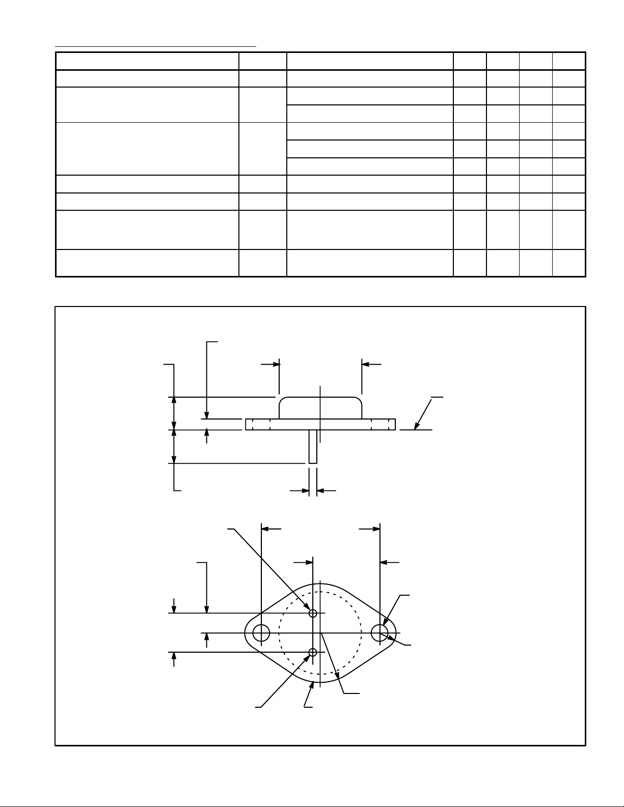
.135 (3.45) Max
.350 (8.89)
.875 (22.2)
Dia Max
= +80°C,
C
– 20 – µs
Cathode
.215 (5.45)
.430
(10.92)
Seating
Plane
.040 (1.02).312 (7.93) Min
1.187 (30.16)
.665
(16.9)
.156 (3.96) Dia
(2 Holes)
.188 (4.8) R Max
.525 (13.35) R Max
Anode/CaseGate
 Loading...