

NTE NTE310P Datasheet
NTE310P
Integrated Thyristor/Rectifier (ITR)
TV Horizontal Deflection & Trace Switch
Absolute Maximum Ratings:
Repetitive Peak Forward Off–State Voltage (TC = +85°C, Note 1), V
Repetitive Peak Reverse Voltage (T
Mean On–State Current (T
= +60°C, 50Hz Sine Wave, Conduction Angle of 180°), IO, I
C
= +85°C, Note 1), V
C
RRM
Rectifier 3.0A. . . . . . . . . . . . . . . . . . . . . . . . . . . . . . . . . . . . . . . . . . . . . . . . . . . . . . . . . . . . . . . . . . . .
SCR 5.0A. . . . . . . . . . . . . . . . . . . . . . . . . . . . . . . . . . . . . . . . . . . . . . . . . . . . . . . . . . . . . . . . . . . . . . .
RMS On–State Current (T
= +60°C, 50Hz Sine Wave, Conduction Angle of 180°), I
C
Rectifier 4.5A. . . . . . . . . . . . . . . . . . . . . . . . . . . . . . . . . . . . . . . . . . . . . . . . . . . . . . . . . . . . . . . . . . . .
SCR 8.0A. . . . . . . . . . . . . . . . . . . . . . . . . . . . . . . . . . . . . . . . . . . . . . . . . . . . . . . . . . . . . . . . . . . . . . .
Surge Current (T
= +85°C, One Full Cycle), I
C
TSM
, I
FSM
60Hz Sinusoidal 80A. . . . . . . . . . . . . . . . . . . . . . . . . . . . . . . . . . . . . . . . . . . . . . . . . . . . . . . . . . . . . .
50Hz Sinusoidal 70A. . . . . . . . . . . . . . . . . . . . . . . . . . . . . . . . . . . . . . . . . . . . . . . . . . . . . . . . . . . . . .
Rate of Change of On–State Current (V
= 700V, IGT = 50mA, tr = 0.1µs), di/dt 200A/µs. . . . . . . . .
D
Peak Forward Gate Power (Negative Gate Bias = –10V, 10µs max, Note 2), P
Peak Reverse Gate Power (Negative Gate Bias = –10V, 10µs max, Note 2), P
Operating Case Temperature Range, T
Storage Temperature Range, T
stg
Maximum Thermal Resistance, Junction–to–Case, R
C
thJC
Lead Temperature (During Soldering, 1/8” from case, 10sec max), T
DRM
L
GM
RGM
F(RMS)
–40° to +85°C. . . . . . . . . . . . . . . . . . . . . . . . . . . . . . . . . . . . .
–40° to +150°C. . . . . . . . . . . . . . . . . . . . . . . . . . . . . . . . . . . . . . . . . .
T(AV)
, I
T(RMS)
2.5°C/W. . . . . . . . . . . . . . . . . . . . . . . . . . . .
800V. . . . . . . . . . . . . . . . . .
750V. . . . . . . . . . . . . . . . . . . . . . . . . .
25W. . . . . . . . . .
25W. . . . . . . .
+225°C. . . . . . . . . . . . . . . . . .
Note 1. These values do not apply if there is a positive gate signal. Gate must be open or negatively
biased.
Note 2. Any p r oduct o f g ate c urrent and gate v oltage w hich r esults i n a g ate p ower l ess than the m axi-
mum i s p ermitted, p rovided t hat t he m aximum r everse g ate b ias (as s pecified) i s n ot exceeded.
Electrical Characteristics:
Parameter Symbol Test Conditions Min Typ Max Unit
Peak Forward Blocking Current I
Instantaneuos Voltage
Rectifier
SCR V
Peak Forward Voltage (Rectifier Only) V
Gate Trigger Current, Continuous DC I
Gate Trigger Voltage, Continuous DC V
(TC = +25°C “Maximum Ratings” unless otherwise specified)
DRM
V
FM
GT
GT
VD = 700V, TC = +85°C – 0.5 1.5 mA
IF = 10A – 1.35 1.7 V
F
IT = 30A – 1.75 3.0 V
T
IFM = 1A – 8 13 V
Anode Voltage = 12V, RL = 30Ω – 15 40 mA
Anode Voltage = 12V, RL = 30Ω – 1.8 4.0 V
Electrical Characteristics (Cont’d): (TC = +25°C “Maximum Ratings” unless otherwise specified)
Parameter Symbol Test Conditions Min Typ Max Unit
Rate of Rise of Off–State Voltage dv/dt VD = 700V, TC = +85°C 175 – – V/µs
Reverse Recovery Time (Rectifier Only) t
Circuit Commutated Turn–Off Time t
IFM = 10A, –diF/dt = –10A/µs, tp = 3µs 0.5 0.7 – µs
rr
Minimum Negative Gate Bias = –20V ,
q
dv/dt = 175V/µs, T
= +80°C, Note 3
C
– – 2.4 µs
Note 3. Turn–off time increases with temperature; therefore, case temperature must not exceed the
level indicated.
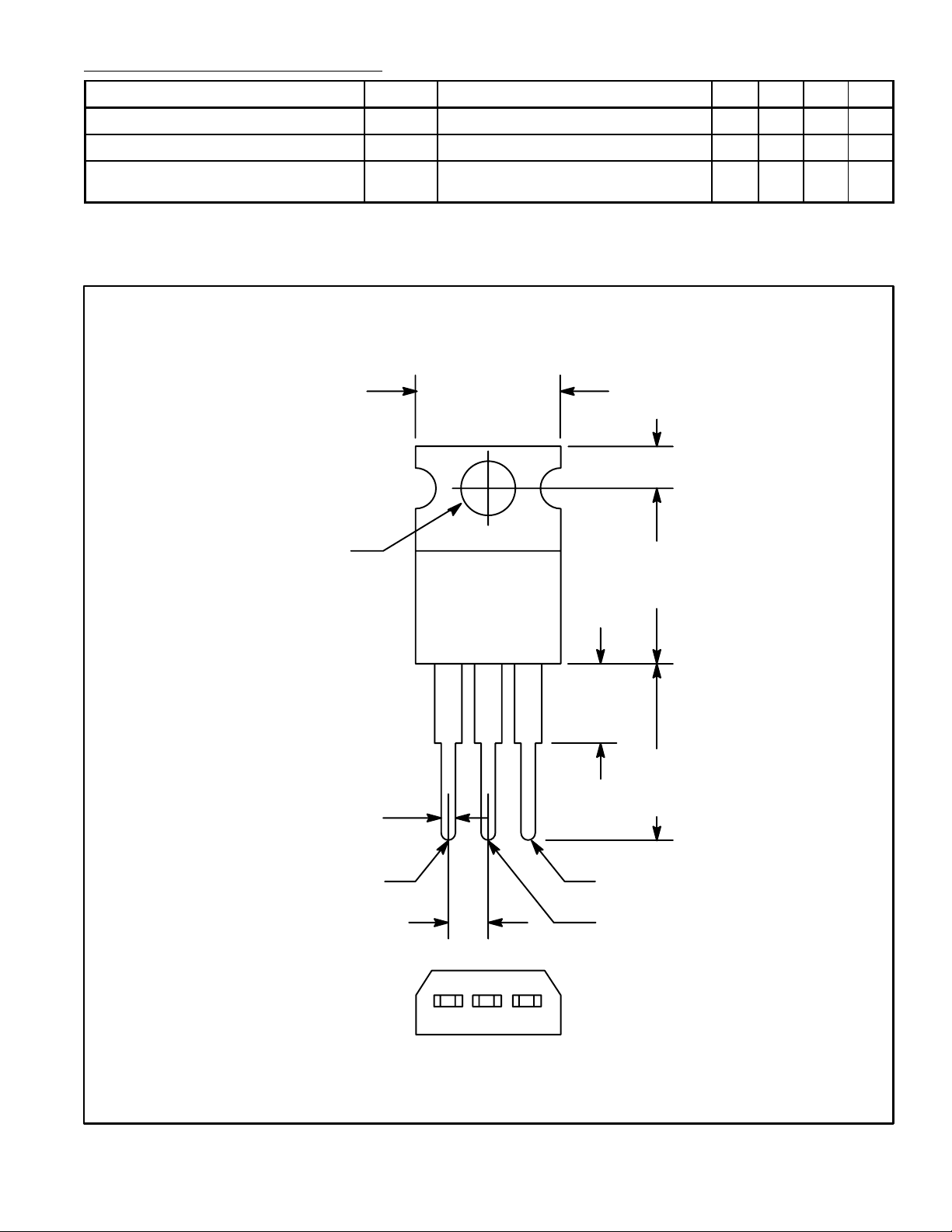
.420 (10.67)
Max
.110 (2.79)
.147 (3.75)
Dia Max
.500
(12.7)
Max
.070 (1.78) Max
Gate
.100 (2.54) Anode/Tab
.250 (6.35)
Max
.500
(12.7)
Min
Cathode
 Loading...