

NTE NTE3102 Datasheet
NTE3102
Photon Coupled Interrupter Module
NPN Transistor
Description:
The NTE3102 Interrupter Module is a gallium arsenide infrared emitting diode coupled to a silicon
phototransistor in a plastic housing. The packaging system is designed to optimize the mechanical
resolution, coupling efficiency, ambient light rejection, cost, and reliability. The gap in the housing provides a means of interrupting the signal with an opaque material, switching the output from an “ON”
into an “OFF” state.
Absolute Maximum Ratings: (TA = +25°C unless otherwise specified)
Total Device
Operating Temperature Range, T
Storage Temperature Range, T
J
stg
Lead Temperature (During Soldering, 5sec Max), T
Infrared Emitting Diode
Forward Current, I
F
Continuous 60mA. . . . . . . . . . . . . . . . . . . . . . . . . . . . . . . . . . . . . . . . . . . . . . . . . . . . . . . . . . . . . . . .
Peak (Pulse Width ≤ 1µs, PRR ≤ 300pps) 3A. . . . . . . . . . . . . . . . . . . . . . . . . . . . . . . . . . . . . . . .
Reverse Voltage, V
Power Dissipation, P
R
E
Derate Above 25°C 1.33mW/°C. . . . . . . . . . . . . . . . . . . . . . . . . . . . . . . . . . . . . . . . . . . . . . . . . . . .
Phototransistor
Power Dissipation, P
D
Derate Above 25°C 2.0mW/°C. . . . . . . . . . . . . . . . . . . . . . . . . . . . . . . . . . . . . . . . . . . . . . . . . . . . .
Continuous Collector Current, I
Collector–Emitter Voltage, V
Emitter–Collector Voltage, V
C
CEO
ECO
L
–55° to +100°C. . . . . . . . . . . . . . . . . . . . . . . . . . . . . . . . . . . . . . . . . .
–55° to +100°C. . . . . . . . . . . . . . . . . . . . . . . . . . . . . . . . . . . . . . . . . .
+260°C. . . . . . . . . . . . . . . . . . . . . . . . . . . . . . . . .
6V. . . . . . . . . . . . . . . . . . . . . . . . . . . . . . . . . . . . . . . . . . . . . . . . . . . . . . . . . . . . . . . . .
100mW. . . . . . . . . . . . . . . . . . . . . . . . . . . . . . . . . . . . . . . . . . . . . . . . . . . . . . . . . . .
150mW. . . . . . . . . . . . . . . . . . . . . . . . . . . . . . . . . . . . . . . . . . . . . . . . . . . . . . . . . . .
100mA. . . . . . . . . . . . . . . . . . . . . . . . . . . . . . . . . . . . . . . . . . . . . . . . . .
55V. . . . . . . . . . . . . . . . . . . . . . . . . . . . . . . . . . . . . . . . . . . . . . . . . . . . . .
6V. . . . . . . . . . . . . . . . . . . . . . . . . . . . . . . . . . . . . . . . . . . . . . . . . . . . . . .
Electrical Characteristics: (TA = +25°C, Note 1 unless otherwise specified)
Parameter Symbol Test Conditions Min Typ Max Unit
Emitter
Reverse Breakdown Voltage V
Forward Voltage V
Reverse Current I
Capacitance C
(BR)RIR
F
R
i
= 10µA 6 – – V
IF = 60mA – – 1.7 V
VR = 5V – – 100 nA
V = 0, f = 1MHz – 30 – pF
Note 1. Stray irradiation can alter values of characteristics. Adequate shielding should be provided.
Electrical Characteristics (Cont’d): (TA = +25°C, Note 1 unless otherwise specified)
Parameter Symbol Test Conditions Min Typ Max Unit
Detector
Collector–Emitter Breakdown Voltage V
Emitter–Collector Breakdown Voltage V
(BR)CEOIC
(BR)ECOIE
Collector Dark Current I
Capacitance C
CEO
ce
= 1mA 55 – – V
= 100µA 6 – – V
VCE = 45V – – 100 nA
VCE = 5V, f = 1MHz – 3.3 5.0 pF
Coupled
Photodiode Current I
CE(on)
VCE = 5V, IF = 5mA 0.15 – – mA
VCE = 5V, IF = 20mA 1.0 – – mA
VCE = 5V, IF = 30mA 1.9 – – mA
Collector–Emitter Saturation Voltage V
Turn–On Time t
Turn–Off Time t
CE(sat)IC
on
off
= 1.8mA, IF = 30mA – – 0.4 V
VCC = 5V, IF = 30mA, RL = 2.5kΩ – 8 – µs
– 50 – µs
Note 1. Stray irradiation can alter values of characteristics. Adequate shielding should be provided.
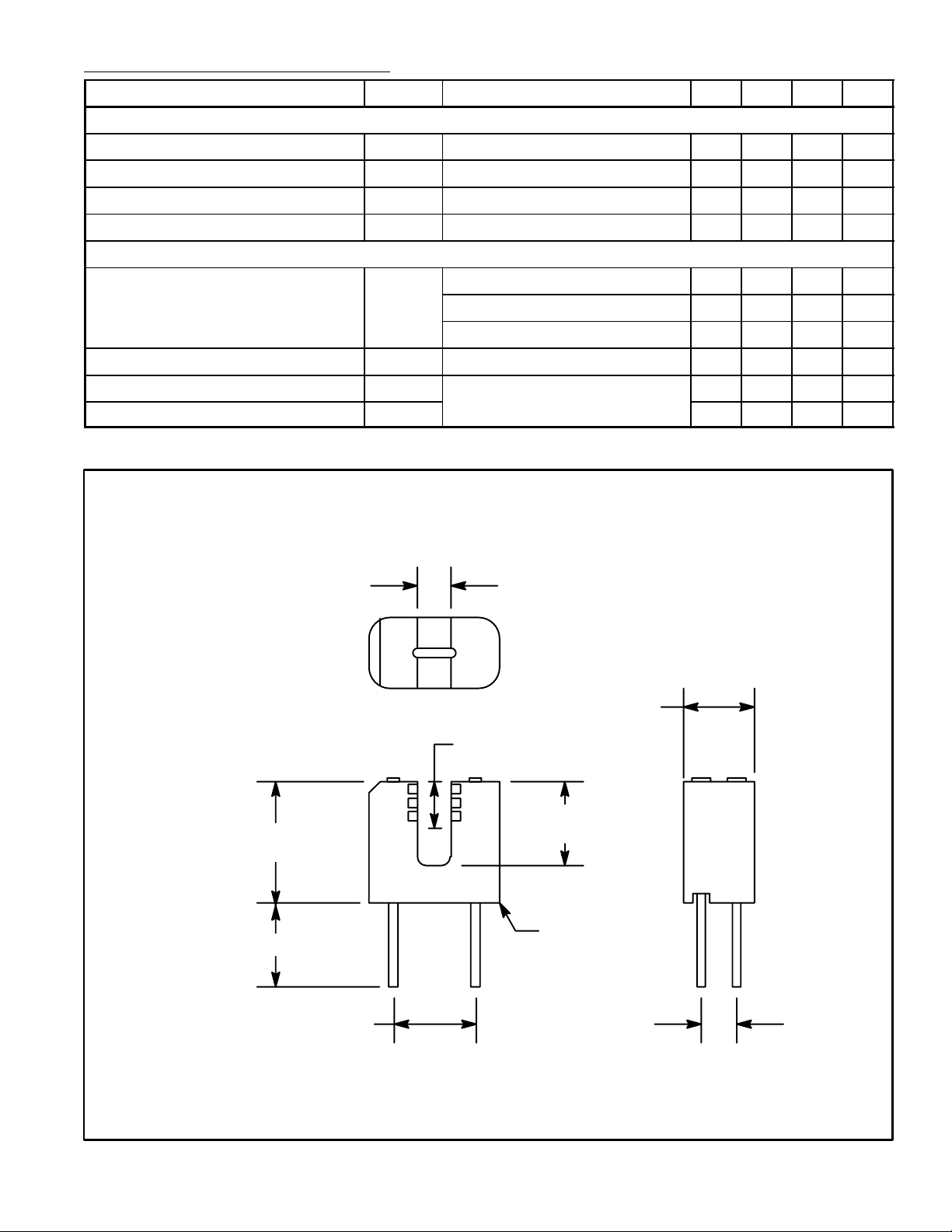
.124 (3.15
.433 (11.0)
Max
.315 (8.0) Min
+
D
D – Detector
E – Emitter
E
+
.246 (6.25)
.136 (3.54) Min
Sensing Area
.303 (7.69)
Min
Seating
Plane
.110 (2.79) Max.295 (7.49) Max
 Loading...