

NTE NTE3097 Datasheet

NTE3097
Optoisolator
Zero Crossing TRIAC Driver
Description:
The NTE3097 is an optoisolator in a 6–Lead DIP type package and contains a gallium arsenide IRED
optically coupled to a monolithic silicon detector performing the function of a Zero Voltage Crossing
bilateral TRIAC Driver . This device is designed for use with a TRIAC in the interface of logic systems
to equipment powered from 240VAC lines such as solid–state relays, industrial controls, motors, solenoids, and consumer appliances, etc.
Features:
D Simplifies Logic Control of 240VAC Power
D Zero Voltage Crossing
D High Breakdown Voltage: V
D High Isolation Voltage: V
ISO
D Small, Economical 6–Lead DIP Package
D dv/dt of 2000V/µs Typ., 1000V/µs Guaranteed
Absolute Maximum Rating: (TA = +25°C unless otherwise specified)
Infrared Emitting Diode
Reverse Voltage, V
R
Continuous Forward Current, I
Total Power Dissipation (TA = +25°C, Negligible Power in Output Driver),P
Derate Above 25°C 1.41mW/°C. . . . . . . . . . . . . . . . . . . . . . . . . . . . . . . . . . . . . . . . . . . . . . . . . . . .
Output Driver
Off–State Output Terminal Voltage, V
Peak Repetitive Surge Current (PW = 100µs, 120pps), I
Total Power Dissipation (TA = +25°C),P
Derate Above 25°C 1.76mW/°C. . . . . . . . . . . . . . . . . . . . . . . . . . . . . . . . . . . . . . . . . . . . . . . . . . . .
Total Device
Isolation Surge Voltage (Peak AC Voltage, 60Hz, 1sec Duration, Note 1), V
Total Power Dissipation (TA = +25°C),P
Derate Above 25°C 2.94mW/°C. . . . . . . . . . . . . . . . . . . . . . . . . . . . . . . . . . . . . . . . . . . . . . . . . . . .
Junction Temperature Range, T
Ambient Operating Temperature Range, T
Storage Temperature Range, T
Lead Temperature (During Soldering, 10sec), T
= 400V Min
DRM
= 7500V Guaranteed
F
DRM
D
D
J
A
stg
L
TSM
D
ISO
6V. . . . . . . . . . . . . . . . . . . . . . . . . . . . . . . . . . . . . . . . . . . . . . . . . . . . . . . . . . . . . . . . .
60mA. . . . . . . . . . . . . . . . . . . . . . . . . . . . . . . . . . . . . . . . . . . . . . . . . . . .
120mW. . . . . . . . . . . .
400V. . . . . . . . . . . . . . . . . . . . . . . . . . . . . . . . . . . . . . . . . . . . .
1A. . . . . . . . . . . . . . . . . . . . . . . . . . . . . .
150mW. . . . . . . . . . . . . . . . . . . . . . . . . . . . . . . . . . . . . . . . . . .
7500V. . . . . . . . . . .
250mW. . . . . . . . . . . . . . . . . . . . . . . . . . . . . . . . . . . . . . . . . . .
–40° to +100°C. . . . . . . . . . . . . . . . . . . . . . . . . . . . . . . . . . . . . . . . . . .
–40° to +85°C. . . . . . . . . . . . . . . . . . . . . . . . . . . . . . . . . . .
–40° to +150°C. . . . . . . . . . . . . . . . . . . . . . . . . . . . . . . . . . . . . . . . . .
+260°C. . . . . . . . . . . . . . . . . . . . . . . . . . . . . . . . . . . .
Note 1. Isolation surge voltage is an internal dielectric breakdown rating. For this test, Pin1 and Pin2
are common, and Pin4, Pin5, and Pin6 are common.
Electrical Characteristics: (TA = +25°C unless otherwise specified)
Parameter Symbol Test Conditions Min Typ Max Unit
Input LED
Reverse Leakage Current I
Forward Voltage V
VR = 6V – 0.05 10 µA
R
IF = 30mA – 1.3 1.5 V
F
Output Detector (IF = 0 unless otherwise specified)
Leakage With LED OFF I
DRM1
Peak On–State Voltage V
Critical Rate of Rise of
dv/dt Note 4 1000 2000 – V/µs
Either Direction, V
Either Direction, ITM = 100mA Peak – 1.8 3.0 V
TM
Off–State Voltage
Coupled
LED Trigger Current,
I
FT
Main Terminal Voltage = 3V, Note 3 – – 15 mA
Current Required to
Latch Output
Holding Current I
Isolation Voltage V
ISO
Either Direction – 100 – µA
H
f = 60Hz, t = 1sec 7500 – – VAC(pk)
Zero Crossing
Inhibit Voltage V
IF = 15mA, MT1–MT2 Voltage Above
IH
Which Device Will Not Trigger
Leakage in Inhibit State I
DRM2IF
= 15mA, V
DRM
= 400V, Note 2 – 2 100 nA
DRM
– 5 20 V
= 400V, Off–State – – 500 µA
Note 2. Test voltage must be applied within dv/dt rating.
Note 3. This device is guaranteed to trigger at an IF1 value less than or equal to max. IFT. Therefore,
recommended operating IF lies between max. IFT (15mA) and absolute max. IF (60mA).
Note 4. This is static dv/dt. Commutating dv/dt is a function of the load–driving thyristor only.
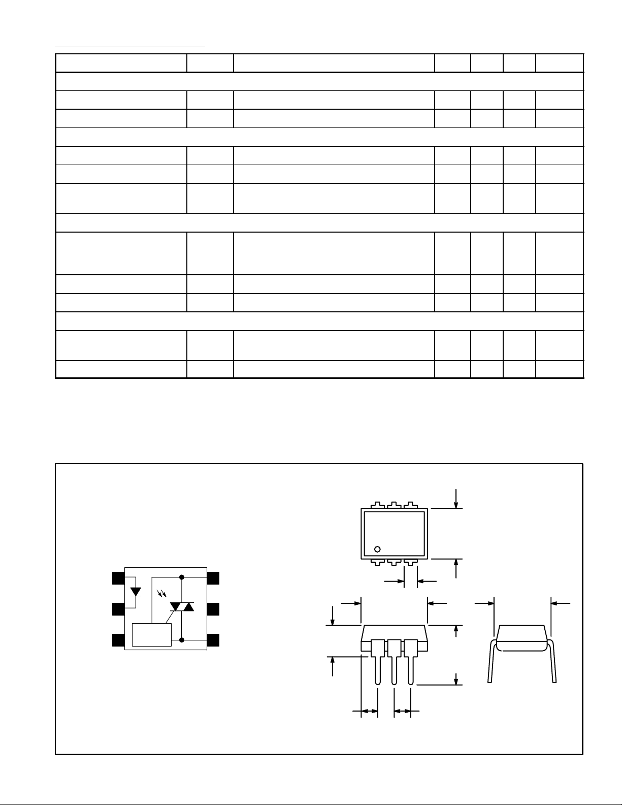
Anode
Cathode
Pin Connection Diagram
6
2
3N.C.
ZERO
CROSSING
CIRCUIT
5
4
Main Terminal1
Substrate
Do Not Connect
Main Terminal
546
123
.070 (1.78)
Max
.350 (8.89)
Max
.200 (5.08)
Max
.260
(6.6)
Max
.300 (7.62)
.350
(8.89)
Max
.085 (2.16)
Max
.100 (2.54)
 Loading...