

NTE NTE3094 Datasheet

NTE3094
Optoisolator
Dual, High Speed, Open Collector NAND Gate
Description:
The NTE3094 consists of a pair of inverting optically coupled gates each with a GaAsP emitting diode
and a unique integrated detector. The photons are collected in the detector by a photodiode and then
amplified by a high gain linear amplifier that drives a Schottky clamped open collector output transistor. each circuit is temperature, current and voltage compensated.
This unique isolator design provides maximum DC and AC circuit isolation between input and output
while achieving LSTTL/TTL circuit compatibility. The isolator operational parameters are guaranteed
from 0° to +70°C, such that a minimum input current of 5mA will sink an eight gate fan–out (13mA)
at the output with 5 volt V
typical propagation delay of 57ns.
Features:
D LSTTL/TTL Compatible: 5V Supply
D Ultra High Speed
D Low Input Current Required
D High Common Mode Rejection
D 3000V DC Withstand Test Voltage
D Typical Data Rate 10M/Bit(s)
applied to the detector. This isolation and coupling is achieved with a
CC
Absolute Maximum Ratings:
(TA = +25°C unless otherwise specified)
Input Diode (Each Channel)
Reverse Voltage, V
Forward Current, I
R
F
Average 15mA. . . . . . . . . . . . . . . . . . . . . . . . . . . . . . . . . . . . . . . . . . . . . . . . . . . . . . . . . . . . . . . . . . .
Peak (≤ 1ms Duration) 30mA. . . . . . . . . . . . . . . . . . . . . . . . . . . . . . . . . . . . . . . . . . . . . . . . . . . . . .
Output Transistor (Each Channel)
Supply Voltage (1 Minute Maximum), V
Output Voltage, V
Output Current, I
Collector Power Dissipation, P
O
O
D
CC
Total Device
Operating Temperature Range, T
Storage Temperature Range, T
opr
stg
Lead Temperature (During Soldering, 1.6mm below seating plane, 10sec Max), T
5V. . . . . . . . . . . . . . . . . . . . . . . . . . . . . . . . . . . . . . . . . . . . . . . . . . . . . . . . . . . . . . . . .
7V. . . . . . . . . . . . . . . . . . . . . . . . . . . . . . . . . . . . . . . . . . . . . .
7V. . . . . . . . . . . . . . . . . . . . . . . . . . . . . . . . . . . . . . . . . . . . . . . . . . . . . . . . . . . . . . . . . .
16mA. . . . . . . . . . . . . . . . . . . . . . . . . . . . . . . . . . . . . . . . . . . . . . . . . . . . . . . . . . . . . . . .
60mW. . . . . . . . . . . . . . . . . . . . . . . . . . . . . . . . . . . . . . . . . . . . . . . . . . . .
0° to +70°C. . . . . . . . . . . . . . . . . . . . . . . . . . . . . . . . . . . . . . . . . . .
–55° to +125°C. . . . . . . . . . . . . . . . . . . . . . . . . . . . . . . . . . . . . . . . . .
L
+260°C. . . . . .
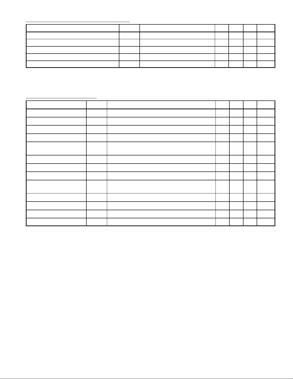
Recommended Operating Conditions:
Parameter Symbol Test Conditions Min Typ Max Unit
Input Current, Low Level (Each Channel) I
Input Current, High Level (Each Channel) I
Supply Voltage, Output V
FL
Note 1 6.3 – 15 mA
FH
CC
0 – 250 µA
4.5 – 5.5 V
Fan Out (TTL Load) N – – 8
Operating Temperature T
A
0 – 70 °C
Note 1. 6.3mA condition permits at least 20% CTR degradation guardband. Initial switching
threshold is 5mA or less.
Electrical Characteristics:
(TA = 0° to +70°C, Note 2 unless otherwise specified)
Parameter Symbol Test Conditions Min Typ Max Unit
High Level Output Current I
Low Level Output Voltage V
High Level Supply Current I
CCH
Low Level Supply Current I
Input–Output Insulation
Leakage Current
Resistance R
Capacitance C
Input Forward Voltage V
Input Reverse Breakdown
V
(BR)RIR
OH
CCL
I
VCC = 5.V, VO = 5.5V, IF = 250µA, Note 3 – 40 250 µA
VCC = 5.5V, IF = 5mA, I
OL
OL(sinking)
= 13mA, Note 3 – 0.4 0.6 V
VCC = 5.V, IF = 0, (Both Channels) – 15 30 mA
VCC = 5.V, IF = 10mA, (Both Channels) – 27 36 mA
Relative Humidity = 45%, TA = +25°C, t = 5s,
IO
IO
IO
F
= 3000V DC, Note 4
V
IO
VIO = 500V, TA = +25°C, Note 4 – 10
f = 1MHz, TA = +25°C, Note 4 – 0.6 – pF
IF = 10mA, TA = +25°C, Note 3, Note 5 – 1.5 1.75 V
– – 1.0 µA
12
= 10µA, TA = +25°C 5 – – V
– Ω
Voltage
Input Capacitance C
VF = 0, f = 1MHz, Note 3 – 60 – pF
IN
Current Transfer Ratio CTR IF = 5mA, RL = 100Ω, Note 6 – 700 – %
Resistance (Input–Input) R
Capacitance (Input–Input) C
VII = 500V, Note 7 – 10
II
f = 1MHz, Note 7 – 0.27 – pF
II
11
– Ω
Note 2. All typicals at TA = +25°C, VCC = 5V unless otherwise specified.
Note 3. Each channel.
Note 4. Measured between Pin1, Pin2, Pin3 and Pin4 shorted together and Pin5, Pin6, Pin7 and
Pin8 shorted together.
Note 5. At 10mA, V
decreases with increasing temperature at the rate of 1.6mV/°C.
F
Note 6. DC Current T ransfer Ratio is defined as the ratio of the output collector current to the forward
bias input current times 100%.
Note 7. Measured between Pin1 and Pin2 shorted together and Pin3 and Pin4 shorted together.
 Loading...