

NTE NTE3092 Datasheet

NTE3092
Optoisolator
Open Collector, NPN Transistor Output
Features:
D High Isolation Voltage
D High Speed: t
D Current Transfer Ratio: 19% Min
Applications:
D Digital Logic Isolation
D Line Receiver Feedback Control
D Power Supply Control
D Switching Power Supply
D Transistor Invertor
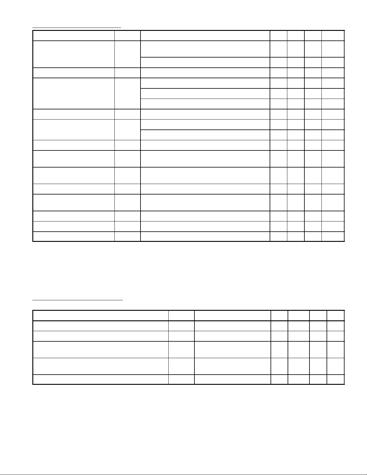
Absolute Maximum Ratings: (TA = +25°C unless otherwise specified)
Input LED
Forward Current, I
Derate Above 70°C 0.8mA/°C. . . . . . . . . . . . . . . . . . . . . . . . . . . . . . . . . . . . . . . . . . . . . . . . . . . . . .
Pulsed Forward Current (Pulse Width = 1ms, Duty Cycle = 50%), I
Derate Above 70°C 1.6mA/°C. . . . . . . . . . . . . . . . . . . . . . . . . . . . . . . . . . . . . . . . . . . . . . . . . . . . . .
Total Pulsed Forward Current (Pulse Width = 1s, 300pps), I
Reverse Voltage, V
Diode Power Dissipation, P
Derate Above 70°C 0.9mW/°C. . . . . . . . . . . . . . . . . . . . . . . . . . . . . . . . . . . . . . . . . . . . . . . . . . . . .
Detector
Output Current, I
Peak Output Current, I
Emitter–Base Reverse Voltage, V
Supply Voltage, V
Output Voltage, V
Base Current, I
B
Output Power Dissipation, P
Derate Above 70°C 2mW/°C. . . . . . . . . . . . . . . . . . . . . . . . . . . . . . . . . . . . . . . . . . . . . . . . . . . . . . .
Coupled
Operating Temperature Range, T
Storage Temperature Range, T
PHL
F
R
O
CC
O
= 0.2µs, t
D
OP
D
= 1.0µs (Typ)
PLH
EB
opr
stg
FP
FPT
25mA. . . . . . . . . . . . . . . . . . . . . . . . . . . . . . . . . . . . . . . . . . . . . . . . . . . . . . . . . . . . . . .
50mA. . . . . . . . . . . . . . . . . . .
1A. . . . . . . . . . . . . . . . . . . . . . . . . . . .
5V. . . . . . . . . . . . . . . . . . . . . . . . . . . . . . . . . . . . . . . . . . . . . . . . . . . . . . . . . . . . . . . . .
45mW. . . . . . . . . . . . . . . . . . . . . . . . . . . . . . . . . . . . . . . . . . . . . . . . . . . . . . .
8mA. . . . . . . . . . . . . . . . . . . . . . . . . . . . . . . . . . . . . . . . . . . . . . . . . . . . . . . . . . . . . . . . .
16mA. . . . . . . . . . . . . . . . . . . . . . . . . . . . . . . . . . . . . . . . . . . . . . . . . . . . . . . . . .
5V. . . . . . . . . . . . . . . . . . . . . . . . . . . . . . . . . . . . . . . . . . . . . . . . . . .
–0.5 to 15V. . . . . . . . . . . . . . . . . . . . . . . . . . . . . . . . . . . . . . . . . . . . . . . . . . . . . . . . .
–0.5 to 15V. . . . . . . . . . . . . . . . . . . . . . . . . . . . . . . . . . . . . . . . . . . . . . . . . . . . . . . . . .
5mA. . . . . . . . . . . . . . . . . . . . . . . . . . . . . . . . . . . . . . . . . . . . . . . . . . . . . . . . . . . . . . . . . .
100mW. . . . . . . . . . . . . . . . . . . . . . . . . . . . . . . . . . . . . . . . . . . . . . . . . . . . .
–55° to +100°C. . . . . . . . . . . . . . . . . . . . . . . . . . . . . . . . . . . . . . . .
–55° to +125°C. . . . . . . . . . . . . . . . . . . . . . . . . . . . . . . . . . . . . . . . . .
Electrical Characteristics: (TA = 0° to +70°C, Note 1 unless otherwise specified)
Parameter Symbol Test Conditions Min Typ Max Unit
Current Transfer Ratio CTR VCC = 4.5V, IF = 16mA, VO = 0.4V, TA = +2 5°C,
Note 2
VCC = 4.5V, IF = 16mA, VO = 0.5V, Note 2 15 21 – %
Logic Low Output Voltage V
Logic High Output Current I
OL
OH
VCC = 4.5V, IF = 16mA, IO = 2.4mA – 0.1 0.4 V
IF = 0mA, VO = VCC = 5.5V, TA = +25°C – 3 500 nA
IF = 0mA, VO = VCC = 15V, TA = +25°C – 0.1 100 µA
IF = 0mA, VO = VCC = 15V – – 250 µA
Logic Low Supply Current I
Logic High Supply Current I
CCLIF
CCHIF
= 16mA, VO = Open, VCC = 15V – 40 – µA
= 0mA, VO = Open, VCC = 15V, TA = +25°C – 0.01 1.0 µA
IF = 0mA, VO = Open, VCC = 15V – – 2.0 µA
Input Forward Voltage V
Temperature Coefficient of
IF = 16mA, TA = +25°C – 1.65 1.7 V
F
IF = 16mA – –1.9 – mV/°C
Forward Voltage
Input Reverse Breakdown
V
(BR)RIR
= 10µA, TA = +25°C 5 – – V
Voltage
Input Capacitance C
Input–Output Insulation
Leakage Current
Resistance (Input–Output) R
Capacitance (Input–Output) C
Transistor DC Current Gain h
I
IN
I–O
I–O
I–O
FE
VF = 0, f = 1MHz – 60 – pF
45% Relative Humidity, t = 5s, V
= 3000Vdc,
I–O
TA = +25°C, Note 3
V
= 500Vdc, Note 3 – 10
I–O
f = 1MHz, Note 3 – 0.6 – pF
VO = 5V, IO = 3mA – 80 –
19 24 – %
– – 1.0 µA
12
– Ω
Note 1. All typicals are at TA = +25°C.
Note 2. DC Current T ransfer Ratio is defined as the ratio of output collector current, IO, to the forward
LED input current, IF, times 100%.
Note 3. Device is considered a two–terminal device: Pin1, Pin2, Pin3, and Pin4 shorted together and
Pin8 shorted together.
Switching Characteristics: (TA = +25°C, VCC = 5V, IF = 16mA, RL = 1.9kΩ unless otherwise
specified)
Parameter Symbol Test Conditions Min Typ Max Unit
Propagation Delay Time to Logic Low at Output t
Propagation Delay Time to Logic High at Output t
Common Mode Transient Immunity at
Logic High Level Output
Common Mode Transient Immunity at
PHL
PLH
CM
CMLVCM = 10V
RL = 1.9kΩ – 0.2 0.8 µs
RL = 1.9kΩ – 0.5 0.8 µs
= 0mA, VCM = 10V
HIF
P–P
,
– 1000 – V/µs
Note 4
, Note 4 – –1000 – V/µs
P–P
Logic Low Level Output
Bandwidth BW RL = 100Ω, Note 5 – 2 – MHz
Note 4. Common mode transient immunity in High Logic level is the maximum tolerable (positivea)
dVcm/dt on the leading edge of the common mode pulse, Vcm, to assure that the output will
remain in a Logic High state (i.e., VO > 2V). Common mode mode transient immunity in the
Logic Low level is the maximum tolerable (negative) dVcm/dt on the trailing edge of the common mode pulse signal, Vcm, to assure that the output will remain in a Logic Low state (i.e.,
VO < 0.8V).
Note 5. The frequency at which the AC output voltage is 3dB below the low frequency asymptote.
 Loading...