

NTE NTE3091 Datasheet
NTE3091
Optoisolator
SCR Output
Description:
The NTE3091 is a gallium arsenide, infrared emitting diode coupled with a light activated silicon
controlled rectifier in a 6–Lead DIP type ppackage.
Absolute Maximum Rating: (TA = +25°C unless otherwise specified)
Infrared Emitting Diode
Reverse Voltage 6V. . . . . . . . . . . . . . . . . . . . . . . . . . . . . . . . . . . . . . . . . . . . . . . . . . . . . . . . . . . . . . . . . . . .
Forward Current
Continuous 60mA. . . . . . . . . . . . . . . . . . . . . . . . . . . . . . . . . . . . . . . . . . . . . . . . . . . . . . . . . . . . . . . .
Peak (Pulse Width = 1µs PPs) 3A. . . . . . . . . . . . . . . . . . . . . . . . . . . . . . . . . . . . . . . . . . . . . . . . . .
LED Power Dissipation 100mW. . . . . . . . . . . . . . . . . . . . . . . . . . . . . . . . . . . . . . . . . . . . . . . . . . . . . . . . . . .
Derate Above 25°C 1.33mW/°C. . . . . . . . . . . . . . . . . . . . . . . . . . . . . . . . . . . . . . . . . . . . . . . . . . . .
Photo–SCR
Peak Forward Voltage 400V. . . . . . . . . . . . . . . . . . . . . . . . . . . . . . . . . . . . . . . . . . . . . . . . . . . . . . . . . . . . .
RMS Forward Current 300mA. . . . . . . . . . . . . . . . . . . . . . . . . . . . . . . . . . . . . . . . . . . . . . . . . . . . . . . . . . .
Peak Forward Current (Pulse Width = 100µs, Duty Cycle = 1%) 10A. . . . . . . . . . . . . . . . . . . . . . . . . .
Surge Current (10ms) 5A. . . . . . . . . . . . . . . . . . . . . . . . . . . . . . . . . . . . . . . . . . . . . . . . . . . . . . . . . . . . . . . .
Reverse Gate Voltage 6V. . . . . . . . . . . . . . . . . . . . . . . . . . . . . . . . . . . . . . . . . . . . . . . . . . . . . . . . . . . . . . .
Power Dissipation (TA = +25°C) 400mW. . . . . . . . . . . . . . . . . . . . . . . . . . . . . . . . . . . . . . . . . . . . . . . . . . .
Derate Above 25°C 5.3mW/°C. . . . . . . . . . . . . . . . . . . . . . . . . . . . . . . . . . . . . . . . . . . . . . . . . . . . .
Power Dissipation (TC = +25°C) 1000mW. . . . . . . . . . . . . . . . . . . . . . . . . . . . . . . . . . . . . . . . . . . . . . . . .
Derate Above 25°C 13.3mW/°C. . . . . . . . . . . . . . . . . . . . . . . . . . . . . . . . . . . . . . . . . . . . . . . . . . . .
Total Device
Isolation Surge Voltage (Input–to–Output)
Peak 3535V. . . . . . . . . . . . . . . . . . . . . . . . . . . . . . . . . . . . . . . . . . . . . . . . . . . . . . . . . . . . . . . . . . . . .
RMS 2500V. . . . . . . . . . . . . . . . . . . . . . . . . . . . . . . . . . . . . . . . . . . . . . . . . . . . . . . . . . . . . . . . . . . . . .
Steady–State Isolation Voltage (Input–to–Output)
Peak 2100V. . . . . . . . . . . . . . . . . . . . . . . . . . . . . . . . . . . . . . . . . . . . . . . . . . . . . . . . . . . . . . . . . . . . .
RMS 1500V. . . . . . . . . . . . . . . . . . . . . . . . . . . . . . . . . . . . . . . . . . . . . . . . . . . . . . . . . . . . . . . . . . . . . .
Operating Temperature Range –55° to +100°C. . . . . . . . . . . . . . . . . . . . . . . . . . . . . . . . . . . . . . . . . . . . .
Storage Temperature Range –55° to +150°C. . . . . . . . . . . . . . . . . . . . . . . . . . . . . . . . . . . . . . . . . . . . . . .
Lead Temperature (During Soldering, 10sec) +260°C. . . . . . . . . . . . . . . . . . . . . . . . . . . . . . . . . . . . . . .
Electrical Characteristics: (TA = +25°C unless otherwise specified)
Parameter Symbol Test Conditions Min Typ Max Unit
Infrared Emitting Diode
Forward Voltage V
Reverse Leakage Current I
Capacitance C
IF = 10mA – 1.2 1.5 V
F
VR = 3V – – 10 µA
R
V = 0, f = 1MHz – 50 – pF
J
Electrical Characteristics (Cont’d): (TA = +25°C unless otherwise specified)
Parameter Symbol Test Conditions Min Typ Max Unit
Photo–SCR
Off–State Voltage V
Reverse Voltage V
On–State Voltage V
Off–State Current I
Reverse Current I
DM
RM
ID = 150µA, RGK = 10kΩ, TA = +100°C 400 – – V
DM
RM
ITM = 0.3A – 1.1 1.3 V
TM
400 – – V
VDM = 400V, RGK = 10kΩ, TA = +100°C – – 150 mA
VRM = 400V, RGK = 10kΩ, TA = +100°C – 20 – mA
Capacitance (Anode–Gate) V = 0, f = 1MHz (Gate–Cathode) – 350 – pF
Coupled
Input Current to Trigger VAK = 50V, RGK = 10kΩ – – 20 mA
VAK = 100V, RGK = 27kΩ – – 11 mA
Isolation Resistance Input–to–Output Voltage = 500V
DC
100 – – GΩ
Input–to–Output Capacitance Input–to–Output Voltage = 0, f = 1MHz – – 2 pF
Coupled dv/dt, Input–to–Output 500 – – V/s
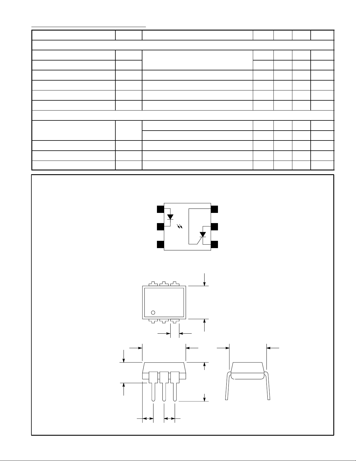
Pin Connection Diagram
Anode
Gate1
6
Cathode
.070 (1.78) Max
.200 (5.08)
Max
2
3N.C.
546
123
.350 (8.89)
Max
.260
(6.6)
Max
.350
(8.89)
Max
5
Anode
Cathode
4
.300 (7.62)
.085 (2.16) Max
.100 (2.54)
 Loading...