

NTE NTE3090 Datasheet

NTE3090
Optoisolator
Schmitt Trigger Output
Description:
The NTE3090 is an optoisolator in a 6–Lead DIP type package and contains a gallium arsenide IRED
optically coupled to a high–speed integrated detector with a Schmitt Trigger output. This device is
designed for applications requiring electrical isolation, fast response time, noise immunity, and digital
logic compatibility.
Features:
D Guaranteed Switching Times: ton, t
D Built–In ON/OFF Threshold Hysteresis
D High Data Rate: 1MHz Typical (NRZ)
D Wide Supply Voltage Capability
D Microprocessor Compatible Drive
Applications:
D Interfacing Computor Terminals to Peripheral
Equipment
D Digital Control of Power Supplies
D Line Receiver – Eliminates Noise
< 4µs
off
D Digital Controls of Motors and Other Servo
Machine Applications
D Logic to Logic Isolator
D Logic Level Shifter – Couples TTL to CMOS
Absolute Maximum Rating: (TA = +25°C unless otherwise specified)
Input LED
Reverse Voltage, V
Forward Current (Note 1), I
R
F
Continuous 60mA. . . . . . . . . . . . . . . . . . . . . . . . . . . . . . . . . . . . . . . . . . . . . . . . . . . . . . . . . . . . . . . .
Peak 1.2A. . . . . . . . . . . . . . . . . . . . . . . . . . . . . . . . . . . . . . . . . . . . . . . . . . . . . . . . . . . . . . . . . . . . . .
LED Power Dissipation (TA = +25°C),P
D
Derate Above 25°C 1.41mW/°C. . . . . . . . . . . . . . . . . . . . . . . . . . . . . . . . . . . . . . . . . . . . . . . . . . . .
Output Detector
Output Voltage Range, V
Supply Voltage Range, V
Output Current, I
O
Detector Power Dissipation (TA = +25°C),P
o
CC
D
Derate Above 25°C 1.76mW/°C. . . . . . . . . . . . . . . . . . . . . . . . . . . . . . . . . . . . . . . . . . . . . . . . . . . .
Total Device
Isolation Surge Voltage (Peak AC Voltage, 60Hz, 1sec Duration, Note 2), V
Total Device Power Dissipation (TA = +25°C),P
D
Derate Above 25°C 2.94mW/°C. . . . . . . . . . . . . . . . . . . . . . . . . . . . . . . . . . . . . . . . . . . . . . . . . . . .
Maximum Operating Temperature Range, T
Storage Temperature Range, T
stg
Lead Temperature (During Soldering, 10sec), T
A
L
ISO
6V. . . . . . . . . . . . . . . . . . . . . . . . . . . . . . . . . . . . . . . . . . . . . . . . . . . . . . . . . . . . . . . . .
120mW. . . . . . . . . . . . . . . . . . . . . . . . . . . . . . . . . . . . . . . . . . . .
0 to 16V. . . . . . . . . . . . . . . . . . . . . . . . . . . . . . . . . . . . . . . . . . . . . . . . . . . . . . .
3 to 16V. . . . . . . . . . . . . . . . . . . . . . . . . . . . . . . . . . . . . . . . . . . . . . . . . . . . .
50mA. . . . . . . . . . . . . . . . . . . . . . . . . . . . . . . . . . . . . . . . . . . . . . . . . . . . . . . . . . . . . . . .
150mW. . . . . . . . . . . . . . . . . . . . . . . . . . . . . . . . . . . . . . . .
7500V. . . . . . . . . . .
250mW. . . . . . . . . . . . . . . . . . . . . . . . . . . . . . . . . . . .
–40° to +85°C. . . . . . . . . . . . . . . . . . . . . . . . . . . . . . . . .
–55° to +150°C. . . . . . . . . . . . . . . . . . . . . . . . . . . . . . . . . . . . . . . . . .
+260°C. . . . . . . . . . . . . . . . . . . . . . . . . . . . . . . . . . . .
Note 1. Pulse Width = 300µs, Duty Cycle = 2%
Note 2. Isolation surge voltage is an internal dielectric breakdown rating. For this test, Pin1 and Pin2
are common, and Pin4, Pin5, and Pin6 are common.
Electrical Characteristics: (TA = 0 to +70°C unless otherwise specified)
I = I ,
Parameter Symbol Test Conditions Min Typ Max Unit
Input LED
Reverse Leakage Current I
Forward Voltage V
Output Detector
Operating Voltage V
Supply Current I
CC(off)IF
Output Current, High I
Coupled
Supply Current I
CC(on)IF
Output Voltage, Low V
Threshold Current, ON I
Threshold Current, OFF I
Hysteresis Ratio
F(on)
F(off)
I
F(on)
I
F(off)
Isolation Voltage V
Turn–On Time t
Fall Time t
Turn–Off Time t
Rise Time t
R
CC
OH
OL
ISO
on
off
r
VR = 3V, RL = 1MΩ – 0.05 10 µA
IF = 10mA – 1.2 1.5 V
F
IF = 0.3mA 0.75 0.95 – V
3 – 15 V
= 0, VCC = 5V – 1 5 mA
IF = 0, VCC = Vo = 15V – – 100 µA
= I
RL = 270Ω, VCC = 5V, IF = I
, VCC = 5V – 1.6 5.0 mA
F(on)
F(on)
– 0.2 0.4 V
RL = 270Ω, VCC = 5V – 1.0 1.6 mA
RL = 270Ω, VCC = 5V 0.3 0.75 – mA
RL = 270Ω, VCC = 5V 0.5 0.75 0.9
60Hz, AC Peak, 1sec, TA = +2 5°C, Note 3 7500 – – V
– 1.2 4 µs
– 0.1 – µs
– 1.2 4 µs
f
RL = 270Ω,
VCC = 5V,
IF = I
T
= +25°C
A
F(on)
,
– 0.1 – µs
AC(pk)
Note 3. Fo r thi s test IRE D Pin1 and Pin2 are common a nd Ou tput Gate Pin4 , Pin 5 , and Pin6 are common.
Anode
Cathode
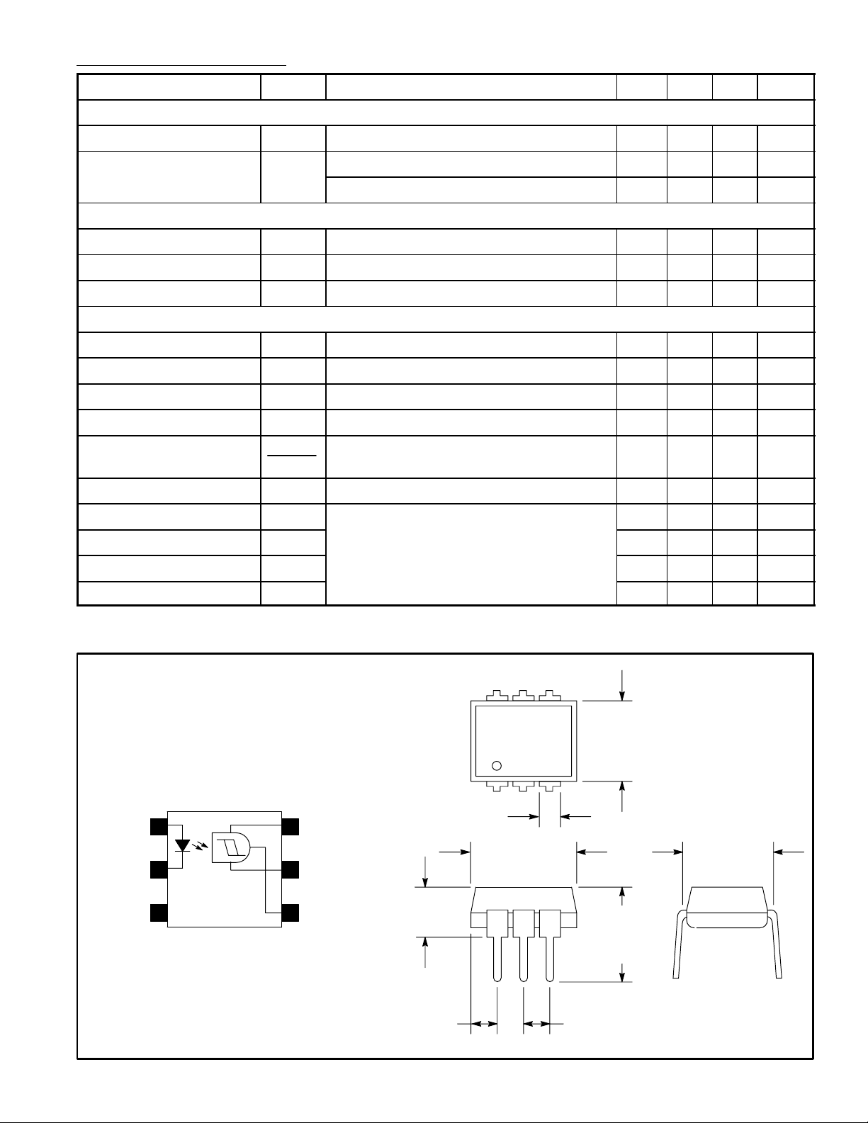
Pin Connection Diagram
1
2
3N.C.
6
5
4
V
CC
GND
V
O
546
123
.070 (1.78) Max
.350 (8.89)
Max
.200 (5.08)
Max
.085 (2.16) Max
.260
(6.6)
Max
.300 (7.62)
.350
(8.89)
Max
.100 (2.54)
 Loading...