

NTE NTE3088 Datasheet

NTE3088
Optoisolator
Silicon NPN High Voltage
Phototransistor Output
Description:
The NTE3088 is a gallium arsenide LED optically coupled to a high voltge, silicon phototransistor in
a 6–Lead DIP type package designed for applications requiring high voltage output. This device is
particularly useful in copy machines and solid state relays.
Features:
D High Voltage: 300V
D High Isolation Voltage: V
Absolute Maximum Ratings: (TA = +25°C, unless otherwise specified)
Input LED
Continuous Forward Current, I
Peak Forward Current (Pulse Width = 1µs, 330pps), I
LED Power Dissipation (TA = +25°C), P
Derate Above 25°C 1.41mW/°C. . . . . . . . . . . . . . . . . . . . . . . . . . . . . . . . . . . . . . . . . . . . . . . . . . . .
= 7500V (Peak)
ISO
F
D
60mA. . . . . . . . . . . . . . . . . . . . . . . . . . . . . . . . . . . . . . . . . . . . . . . . . . . .
F
1.2A. . . . . . . . . . . . . . . . . . . . . . . . . . . . . . . . .
120mW. . . . . . . . . . . . . . . . . . . . . . . . . . . . . . . . . . . . . . . . . . .
Output Transistor
Collector–Emitter Voltage, V
Collector–Base Voltage, V
Emitter–Collector Voltage, V
Continuous Collector Current, I
Detector Power Dissipation (TA = +25°C), P
CER
CBO
ECO
C
D
Derate Above 25°C 1.76mW/°C. . . . . . . . . . . . . . . . . . . . . . . . . . . . . . . . . . . . . . . . . . . . . . . . . . . .
Total Device
Isolation Surge Voltage (Peak AC Voltage, 60Hz, 1sec Duration, Note 1), V
Total Device Power Dissipation (TA = +25°C), P
D
ISO
Derate Above 25°C 2.94mW/°C. . . . . . . . . . . . . . . . . . . . . . . . . . . . . . . . . . . . . . . . . . . . . . . . . . . .
Operating Temperature Range, T
Storage Temperature Range, T
Lead Temperature (During Soldering for 10sec), T
J
–55° to +150°C. . . . . . . . . . . . . . . . . . . . . . . . . . . . . . . . . . . . . . . . . .
stg
L
Note 1. Isolation surge voltage is an internal device dielectric breakdown rating.
300V. . . . . . . . . . . . . . . . . . . . . . . . . . . . . . . . . . . . . . . . . . . . . . . . . . . . .
300V. . . . . . . . . . . . . . . . . . . . . . . . . . . . . . . . . . . . . . . . . . . . . . . . . . . . . .
7V. . . . . . . . . . . . . . . . . . . . . . . . . . . . . . . . . . . . . . . . . . . . . . . . . . . . . . .
100mA. . . . . . . . . . . . . . . . . . . . . . . . . . . . . . . . . . . . . . . . . . . . . . . . . .
150mW. . . . . . . . . . . . . . . . . . . . . . . . . . . . . . . . . . . . . . .
7500V. . . . . . . . . . .
250mW. . . . . . . . . . . . . . . . . . . . . . . . . . . . . . . . . . . .
–55° to +100°C. . . . . . . . . . . . . . . . . . . . . . . . . . . . . . . . . . . . . . . . . .
+260°C. . . . . . . . . . . . . . . . . . . . . . . . . . . . . . . . . .
Electrical Characteristics: (TA = +25°C unless otherwise specified)
Parameter Symbol Test Conditions Min Typ Max Unit
Input LED
Reverse Leakage Current I
Forward Voltage V
R
VR = 6V – – 10 µA
IF = 10mA – 1.2 1.5 V
F
Capacitance C VR = 0, f = 1MHz – 18 – pF
Photodarlington (IF = 0 unless otherwise specified)
Collector–Emitter Dark Current I
CER
VCE = 200V, RBE = 1MΩ – – 100 nA
VCE = 200V, RBE = 1MΩ, TA = +1 00°C – – 250 µA
Collector–Base Breakdown Voltage V
Collector–Emitter Breakdown Voltage V
Emitter–Base Breakdown Voltage V
(BR)CBOIC
(BR)CERIC
(BR)EBOIE
= 100µA – – 300 V
= 1mA, RBE = 1MΩ – – 300 V
= 100µA 5 – – V
Coupled
Current Transfer Ratio CTR VCE = 10V, IF = 10mA, RBE = 1MΩ 20 – – %
Isolation Surge Voltage V
Isolation Resistance R
Collector–Emitter Saturation Voltage V
Isolation Capacitance C
ISO
ISO
CE(sat)IC
ISO
60Hz Peak AC, 1sec, Note 2 7500 – – V
V = 500V, Note 2 – 10
11
–
Ω
= 0.5mA, IF = 10mA, RBE = 1MΩ – – 0.4 V
V = 0, f = 1MHz, Note 2 – 0.2 – pF
Switching
Turn–On Time t
Turn–Off Time t
on
off
VCC = 10V, IF = 5mA, RL = 100Ω
– 5 – µs
– 5 – µs
Note 2. For this test LED Pin1 and Pin2 are common and phototransistor Pin4, Pin5, and Pin6 are
common.
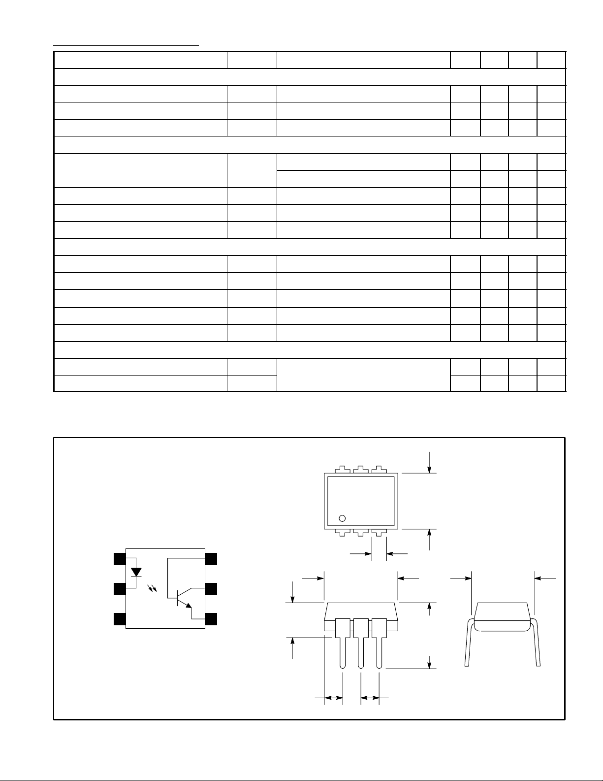
Anode
Cathode
Pin Connection Diagram
6
2
3N.C.
5
4
Base1
Collector
Emitter
546
123
.070 (1.78) Max
.350 (8.89)
Max
.200 (5.08)
Max
.260
(6.6)
Max
.300 (7.62)
.350
(8.89)
Max
.085 (2.16) Max
.100 (2.54)
 Loading...