

NTE NTE3083 Datasheet
NTE3083
Optoisolator
NPN Darlington Transistor Output
Description:
The NTE3083 contains a gallium arsenide infrared emitter optically coupled to a silicon planer photo–
darlington in a 6–Lead DIP type package.
Features:
D High Sensitivity: 1mA on the Input will Sink a TTL gate
12
D High Isolation: 3550VDC, 10
Absolute Maximum Ratings:
Storage Temperature Range, T
Operating Temperature Range, T
Lead Temperature (During Soldering, 10sec), T
Total Power Dissipation (T
= +25°C), P
A
Derate Linearly to 100°C 3.3mW/°C. . . . . . . . . . . . . . . . . . . . . . . . . . . . . . . . . . . . . . . . . . . . . . . .
Input to Output Isolation Voltage (1sec), V
Ω, 0.5pF
stg
opr
D
ISOL
–65° to +150°C. . . . . . . . . . . . . . . . . . . . . . . . . . . . . . . . . . . . . . . . . .
–55° to +100°C. . . . . . . . . . . . . . . . . . . . . . . . . . . . . . . . . . . . . . . .
L
+260°C. . . . . . . . . . . . . . . . . . . . . . . . . . . . . . . . . . . .
250mW. . . . . . . . . . . . . . . . . . . . . . . . . . . . . . . . . . . . . . . . . .
3550VDC. . . . . . . . . . . . . . . . . . . . . . . . . . . . . . . . . . . .
Input Diode
Forward Current, I
Reverse Voltage, V
F
R
Peak Forward Current (1µs pulse, 300pps), I
Output Darlington
Collector–Emitter Voltage, V
Collector–Base Voltage, V
Emitter–Base Voltage, V
Collector Current, I
C
Electro–Optical Characteristics:
Parameter Symbol Test Conditions Min Typ Max Unit
Isolation Between Emitter and Detector
Capacitance C
Resistance R
Voltage Breakdown V
CEO
CBO
EBO
(TA = +25°C unless otherwise specified)
iso
iso
iso
60mA. . . . . . . . . . . . . . . . . . . . . . . . . . . . . . . . . . . . . . . . . . . . . . . . . . . . . . . . . . . . . . .
peak 3A. . . . . . . . . . . . . . . . . . . . . . . . . . . . . . . . . . . . . .
F
30V. . . . . . . . . . . . . . . . . . . . . . . . . . . . . . . . . . . . . . . . . . . . . . . . . . . . . .
30V. . . . . . . . . . . . . . . . . . . . . . . . . . . . . . . . . . . . . . . . . . . . . . . . . . . . . . .
125mA. . . . . . . . . . . . . . . . . . . . . . . . . . . . . . . . . . . . . . . . . . . . . . . . . . . . . . . . . . . . .
f = 1MHz – 0.5 – pF
V = 500VDC 101110
t = 1sec 3550 – – VDC
12
– Ω
3V. . . . . . . . . . . . . . . . . . . . . . . . . . . . . . . . . . . . . . . . . . . . . . . . . . . . . . . . . . . . . . . . .
6V. . . . . . . . . . . . . . . . . . . . . . . . . . . . . . . . . . . . . . . . . . . . . . . . . . . . . . . . . .
Electro–Optical Characteristics (Cont’d): (TA = +25°C unless otherwise specified)
Parameter Symbol Test Conditions Min Typ Max Unit
Emitter (GaAs LED)
Forward Voltage V
Reverse Voltage V
Junction Capacitance C
Detector (Silicon Photo–Darlington)
Collector Breakdown Voltage V
Base Breakdown Voltage V
Emitter Breakdown Voltage V
Collector Leakage Current I
Saturation Voltage V
(BR)CEOIC
(BR)CBOIC
(BR)EBOIE
CEO
CE(sat)IC
Base Photo–Current I
Darlington Gain h
Collector–Emitter Capacitance C
FE
CE
Switching Times, Coupled
Rise Time, Fall Time tr, t
TTL Gate Turn–On Time t
TTL Gate Turn–Off Time t
DC Collector Current Transfer
ON
OFF
CTR IF = 10mA, VCE = 5V 200 400 – %
Ratio
IF = 20mA – 1.15 1.50 V
F
IR = 10µA 3.0 25.0 – V
R
VR = 0V – 50 – pF
J
= 1mA 30 60 – V
= 10µA 30 60 – V
= 10µA 6 8 – V
VCE = 10V – 1 100 nA
= 2mA, IF = 1mA – 0.8 1.0 V
IC = 10mA, IF = 5mA – 0.8 1.0 V
IC = 50mA, IF = 10mA – 0.9 1.2 V
B
VCB = 5V, IF = 10mA – 2 – µA
IB = 1µA, VCE = 1V – 50k –
VCE = 10V – 6 – pF
VCC = 10V, IC = 10mA, RL = 100Ω – 80 – µs
f
IF = 1mA – 200 – µs
IF = 1mA – 400 – µs
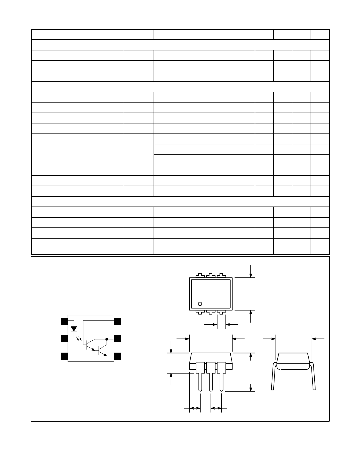
Anode
Cathode
546
123
1
2
3N.C.
Base
6
5
Collector
Emitter
4
.070 (1.78) Max
.350 (8.89)
Max
.200 (5.08)
Max
.085 (2.16) Max
.260
(6.6)
Max
.300 (7.62)
.350
(8.89)
Max
.100 (2.54)
 Loading...