

NTE NTE3047 Datasheet

NTE3047
Optoisolator
TRIAC Driver Output
Description:
The NTE3047 optoisolator consists of a gallium arsenide infrared emitting diode, optically coupled
to a silicon bilateral switch and is designed for applications requiring isolated TRIAC triggering, low
current isolated AC switching, high electrical isolation (to 7500V peak), high detector standoff voltage,
small size, and low cost.
Applications:
D Solenoid/Valve Controls
D Lamp Ballasts
D Motor Controls
D Static AC Power Switch
Absolute Maximum Ratings: (TA = +25°C unless otherwise specified)
Infrared Emitting Diode
Reverse Voltage, V
Continuous Forward Current, I
R
F
Total Power Dissipation (TA = +25°C, Negligible Power in Transistor), P
Derate Above 25°C 1.33mW/°C. . . . . . . . . . . . . . . . . . . . . . . . . . . . . . . . . . . . . . . . . . . . . . . . . . . .
D Solid State Relays
D Incandescent lamp Dimmers
D Interfacing Microprocessors to 115VAC
Preipherals
D
3V. . . . . . . . . . . . . . . . . . . . . . . . . . . . . . . . . . . . . . . . . . . . . . . . . . . . . . . . . . . . . . . . .
60mA. . . . . . . . . . . . . . . . . . . . . . . . . . . . . . . . . . . . . . . . . . . . . . . . . . . .
100mW. . . . . . . . . . . . . . .
Output Driver
Off–State Output Terminal Voltage, V
Peak Repetitive Surge Current (PW = 1ms, 120pps), I
Total Power Dissipation (TA = +25°C), P
DRM
TSM
D
Derate Above 25°C 4mW/°C. . . . . . . . . . . . . . . . . . . . . . . . . . . . . . . . . . . . . . . . . . . . . . . . . . . . . . .
Total Device
Isolation Surge Voltage (Peak AC Voltage, 60Hz, 5sec Duration, Note 1), V
Total Power Dissipation (TA = +25°C), P
D
Derate Above 25°C 4.4mW/°C. . . . . . . . . . . . . . . . . . . . . . . . . . . . . . . . . . . . . . . . . . . . . . . . . . . . .
Junction Temperature Range, T
Operating Ambient Temperature Range, T
Storage Temperature Range, T
Lead Temperature (During Soldering, 10s), T
Note 1. Isolation surge voltage, V
J
stg
A
L
, is an internal device dielectric breakdown rating. For this test,
ISO
Pin1 and Pin2 are common, and Pin4, Pin5, and Pin6 are common.
ISO
250V. . . . . . . . . . . . . . . . . . . . . . . . . . . . . . . . . . . . . . . . . . . . .
1A. . . . . . . . . . . . . . . . . . . . . . . . . . . . . . . .
300mW. . . . . . . . . . . . . . . . . . . . . . . . . . . . . . . . . . . . . . . . . . .
7500VAC. . . . . . . .
330mW. . . . . . . . . . . . . . . . . . . . . . . . . . . . . . . . . . . . . . . . . . .
–40° to +100°C. . . . . . . . . . . . . . . . . . . . . . . . . . . . . . . . . . . . . . . . . . .
–40° to +85°C. . . . . . . . . . . . . . . . . . . . . . . . . . . . . . . . . . .
–40° to +150°C. . . . . . . . . . . . . . . . . . . . . . . . . . . . . . . . . . . . . . . . . .
+260°C. . . . . . . . . . . . . . . . . . . . . . . . . . . . . . . . . . . . . .
Electrical Characteristics: (TA = +25°C unless otherwise specified)
Parameter Symbol Test Conditions Min Typ Max Unit
Input LED
Reverse Leakage Current I
Forward Voltage V
VR = 3V – 0.05 100 µA
R
IF = 10mA – 1.15 1.5 V
F
Output Detector (IF = 0 unless otherwise specified)
Peak Blocking Current , Either Direction I
Peak On–State Voltage, Either Direction V
DRM
TM
Rated V
, Note 2 – 10 100 nA
DRM
ITM = 100mA Peak – 1.8 3.0 V
Critical Rate of Rise of Off–State Voltage dv/dt Note 3 – 10 – V/µs
Coupled
LED T rigger Current, Current Required to
Latch Output
Holding Current, Either Direction I
I
FT
Main Terminal Voltage = 3V,
– 8 15 mA
Note 4
H
– 100 – µA
Note 2. Test voltage must be applied within dv/dt rating.
Note 3. This is static dv/dt. Commutating dv/dt is a function of the load–driving thyristor(s) only.
Note 4. This device is guaranteed to trigger at an IF value les than or equal to max. IFT. Therefore,
recommended operating IF lies between max. IFT (15mA) and absolute max. IF (60mA).
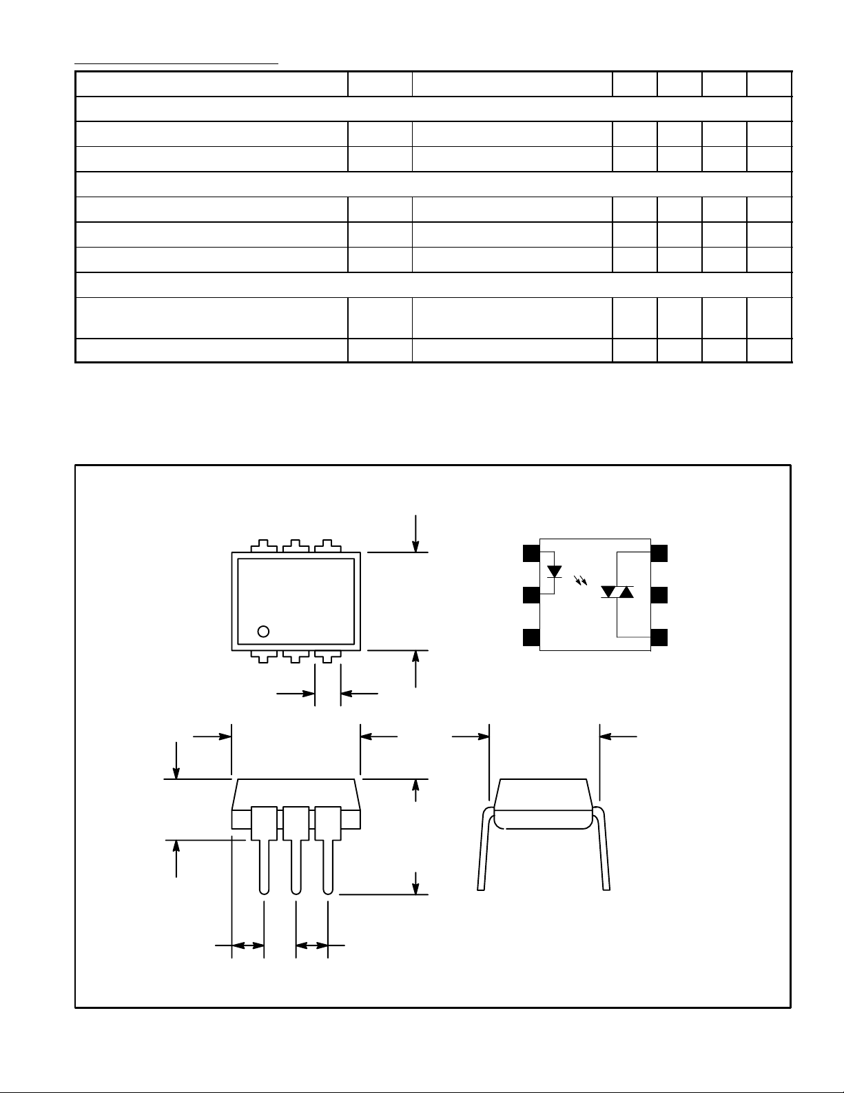
.070 (1.78) Max
.200 (5.08)
Max
.085 (2.16) Max
546
123
.350 (8.89)
Max
.100 (2.54)
.260
(6.6)
Max
.350
(8.89)
Max
Anode
Cathode
2
3N.C.
.300 (7.62)
Main Terminal1
6
TRIAC Driver
54Substrate
Do Not Connect
Main Terminal
 Loading...