

NTE NTE3046 Datasheet

NTE3046
Optoisolator
SCR Photothyristor Output
Description:
The NTE3046 consists of a photo SCR coupled to a gallium arsenide infrared diode in a 6–Lead DIP
type plastic package.
Features:
D Built–In Memory
D AC Switch (SPST)
D High Current Carrying Capability
Absolute Maximum Ratings:
LED (GaAs Diode)
Reverse Voltage 3V. . . . . . . . . . . . . . . . . . . . . . . . . . . . . . . . . . . . . . . . . . . . . . . . . . . . . . . . . . . . . . . . . . . .
Forward Current
Continuous 60mA. . . . . . . . . . . . . . . . . . . . . . . . . . . . . . . . . . . . . . . . . . . . . . . . . . . . . . . . . . . . . . . .
Peak (50µs pulse, 120 pps) 500mA. . . . . . . . . . . . . . . . . . . . . . . . . . . . . . . . . . . . . . . . . . . . . . . . .
Power Dissipation (TA = +25°C) 90mW. . . . . . . . . . . . . . . . . . . . . . . . . . . . . . . . . . . . . . . . . . . . . . . . . . . .
Derate Linearly Above 25°C 1.2mW/°C. . . . . . . . . . . . . . . . . . . . . . . . . . . . . . . . . . . . . . . . . . . . .
Detector (Photo SCR)
DC Anode Current 100mA. . . . . . . . . . . . . . . . . . . . . . . . . . . . . . . . . . . . . . . . . . . . . . . . . . . . . . . . . . . . . . .
Peak Pulse Current (100µs pulse, 120 pps) 1.0A. . . . . . . . . . . . . . . . . . . . . . . . . . . . . . . . . . . . . . . . . . .
Average Gate Current 25mA. . . . . . . . . . . . . . . . . . . . . . . . . . . . . . . . . . . . . . . . . . . . . . . . . . . . . . . . . . . .
Reverse Gate Current 1.0mA. . . . . . . . . . . . . . . . . . . . . . . . . . . . . . . . . . . . . . . . . . . . . . . . . . . . . . . . . . . .
Anode Voltage (DC or Peak AC) 400V. . . . . . . . . . . . . . . . . . . . . . . . . . . . . . . . . . . . . . . . . . . . . . . . . . . .
Power Dissipation (TA = +25°C) 200mW. . . . . . . . . . . . . . . . . . . . . . . . . . . . . . . . . . . . . . . . . . . . . . . . . . .
Derate Linearly Above 25°C 2.67mW/°C. . . . . . . . . . . . . . . . . . . . . . . . . . . . . . . . . . . . . . . . . . . .
Total Device
Isolation Surge Voltage 3550V. . . . . . . . . . . . . . . . . . . . . . . . . . . . . . . . . . . . . . . . . . . . . . . . . . . . . . . . . . .
Power Dissipation (TA = +25°C) 250mW. . . . . . . . . . . . . . . . . . . . . . . . . . . . . . . . . . . . . . . . . . . . . . . . . . .
Derate Linearly Above 25°C 3.3mW/°C. . . . . . . . . . . . . . . . . . . . . . . . . . . . . . . . . . . . . . . . . . . . .
Operating Temperature Range –30° to +100°C. . . . . . . . . . . . . . . . . . . . . . . . . . . . . . . . . . . . . . . . . . . . .
Storage Temperature Range –55° to +150°C. . . . . . . . . . . . . . . . . . . . . . . . . . . . . . . . . . . . . . . . . . . . . . .
Lead Temperature (During Soldering for 7sec) +260°C. . . . . . . . . . . . . . . . . . . . . . . . . . . . . . . . . . . . . .
Electrical Characteristics: (TA = +25°C unless otherwise specified)
Parameter Symbol Test Conditions Min Typ Max Unit
Input Diode
Forward Voltage V
Reverse Voltage V
Junction Capacitance C
F
R
J
Detector
Forward Leakage Current I
Reverse Leakage Current I
Forward Blocking Voltage V
Reverse Blocking Voltage V
ON Voltage V
Holding Current I
Gate Trigger Voltage V
Gate Trigger Current I
FSM
FX
RX
, V
ROM
TM
HX
GT
GT
Coupled
Turn–On Current (Threshold) I
Switching tr + t
FT
d
Steady State Voltage t = 1min 3500 – – V
Surge Isolation Rating V
Isolation Resistance R
Isolation Capacitance C
ISO
ISO
ISO
IF = 20mA – 1.25 1.5 V
IR = 10µA 3.0 – – V
VR = 0 – 50 – pF
VFX = Rated VFX, RGK = 27kΩ – 0.02 2.0 µA
VRX = Rated VRX, RGK = 27kΩ – 0.02 2.0 µA
RGK = 10kΩ, TA = +100°C 400 – – V
DM
400 – – V
IT = 100mA – 0.98 1.3 V
RGK = 27kΩ 0.01 0.16 0.50 mA
VFX = 100V – 0.6 1.0 V
VFX = 100V, RL = 10kΩ, RGK = 27kΩ – 23 100 µA
VFX = 100V, RGK = 27kΩ 0.5 5.0 14.0 mA
VCC = 20V, IF = 30mA, RGK = 27kΩ – 7 – µs
t = 1min 2500 – – V
t = 1sec 4000 – – V
t = 1sec 3000 – – V
V = 500V 10
11
10
12
f = 1MHz – 1 2 pF
– Ω
rms
rms
Anode
Cathode
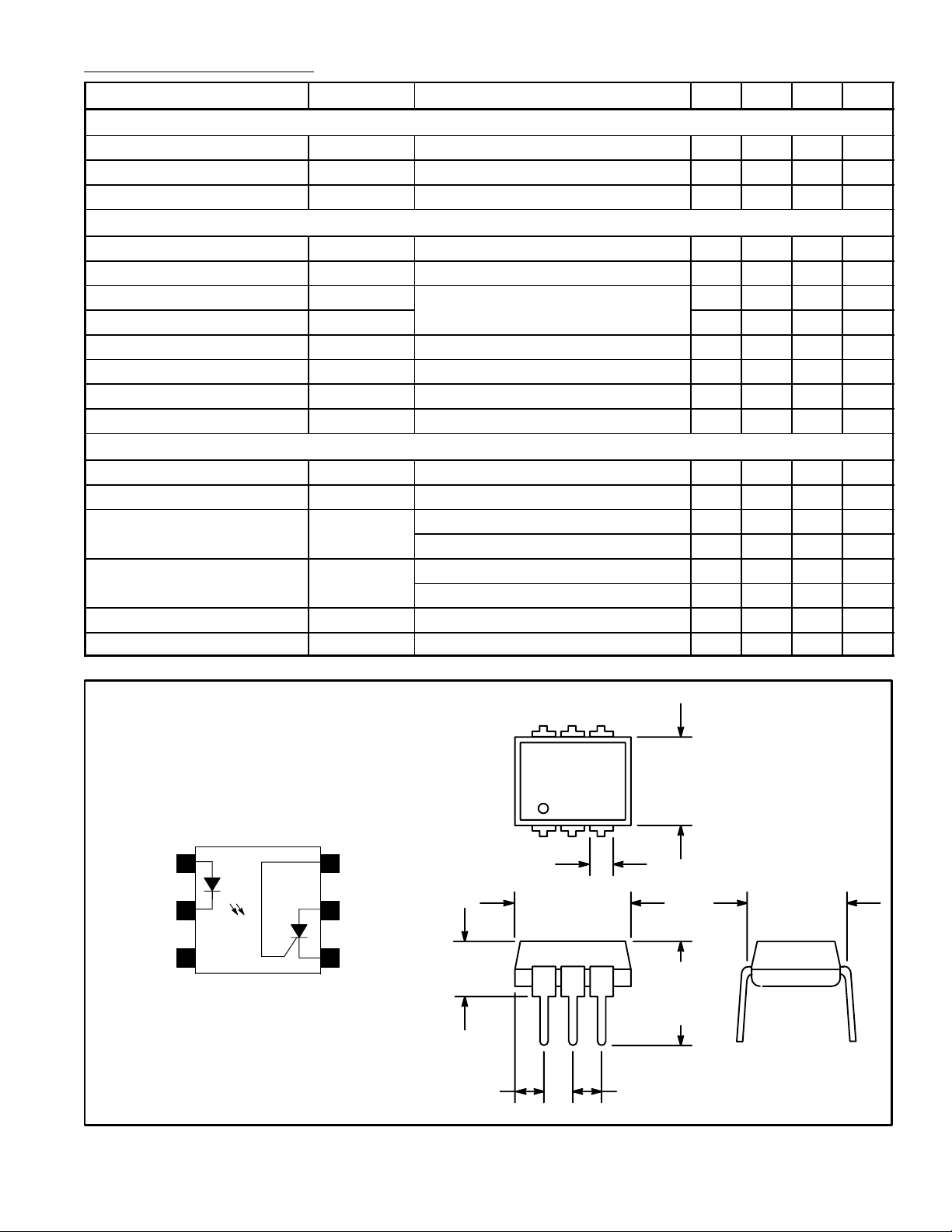
Pin Connection Diagram
6
2
3N.C.
5
4
Gate1
Anode
Cathode
.085 (2.16) Max
.070 (1.78) Max
.200 (5.08)
Max
546
123
.350 (8.89)
Max
.100 (2.54)
.260
(6.6)
Max
.300 (7.62)
.350
(8.89)
Max
 Loading...