

NTE NTE3040 Datasheet
NTE3040
Optoisolator
NPN Transistor Output
Description:
The NTE3040 is a gallium arsenide, infrared emitting diode in a 6–Lead DIP type package coupled
with a silicon phototransistor.
Absolute Maximum Ratings: (TA = +25°C, unless otherwise specified)
Infrared Emitting Diode
Power Dissipation, P
D
Derate above 25°C ambient 2.6mW/°C. . . . . . . . . . . . . . . . . . . . . . . . . . . . . . . . . . . . . . . . . . . . .
Forward Current (Continuous), I
Forward Current (Peak), I
C
(Pulse Width 1µsec, 300pps)
Reverse Voltage, V
R
Phototransistor
Power Dissipation, P
D
Derate above 25°C ambient 2.6mW/°C. . . . . . . . . . . . . . . . . . . . . . . . . . . . . . . . . . . . . . . . . . . . .
Collector to Emitter Voltage, V
Collector to Base Voltage, V
Emitter to Collector Voltage, V
CEO
CBO
ECO
Collector Current (Continuous), I
C
C
200mW. . . . . . . . . . . . . . . . . . . . . . . . . . . . . . . . . . . . . . . . . . . . . . . . . . . . . . . . . . .
60mA. . . . . . . . . . . . . . . . . . . . . . . . . . . . . . . . . . . . . . . . . . . . . . . . . . .
3A. . . . . . . . . . . . . . . . . . . . . . . . . . . . . . . . . . . . . . . . . . . . . . . . . . . . . . . . . . .
3V. . . . . . . . . . . . . . . . . . . . . . . . . . . . . . . . . . . . . . . . . . . . . . . . . . . . . . . . . . . . . . . . .
200mW. . . . . . . . . . . . . . . . . . . . . . . . . . . . . . . . . . . . . . . . . . . . . . . . . . . . . . . . . . .
30V. . . . . . . . . . . . . . . . . . . . . . . . . . . . . . . . . . . . . . . . . . . . . . . . . . . .
70V. . . . . . . . . . . . . . . . . . . . . . . . . . . . . . . . . . . . . . . . . . . . . . . . . . . . . .
7V. . . . . . . . . . . . . . . . . . . . . . . . . . . . . . . . . . . . . . . . . . . . . . . . . . . . .
100mA. . . . . . . . . . . . . . . . . . . . . . . . . . . . . . . . . . . . . . . . . . . . . . . . .
Total Device
Storage Temperature, T
stg
Operating Temperature, T
opr
–55° to +150°C. . . . . . . . . . . . . . . . . . . . . . . . . . . . . . . . . . . . . . . . . . . . . . . . .
–55° to +100°C. . . . . . . . . . . . . . . . . . . . . . . . . . . . . . . . . . . . . . . . . . . . . . .
Lead Soldering Temperature (10 seconds) +260°C. . . . . . . . . . . . . . . . . . . . . . . . . . . . . . . . . . . . . . . . . .
Surge Isolation Voltage (Input to Output)
(Peak) 1500V. . . . . . . . . . . . . . . . . . . . . . . . . . . . . . . . . . . . . . . . . . . . . . . . . . . . . . . . . . . . . . . . . . . .
(RMS) 1060V. . . . . . . . . . . . . . . . . . . . . . . . . . . . . . . . . . . . . . . . . . . . . . . . . . . . . . . . . . . . . . . . . . . .
Electrical Characteristics: (TA = +25°C, unless otherwise specified)
Parameter Symbol Test Conditions Min Typ Max Unit
Infrared Emitting Diode
Forward Voltage V
Reverse Current I
Capacitance C
R
IF = 10mA – 1.1 1.5 V
F
VR = 3V – – 10 mA
V = 0, f = 1MH
J
Z
– 50 – pf
Electrical Characteristics (Cont’d): (TA = +25°C, unless otherwise specified)
Parameter Symbol Test Conditions Min Typ Max Unit
Phototransistor
Collector–Emitter Breakdown Voltage V
Collector–Base Breakdown Voltage V
Emitter–Collector Breakdown Voltage V
Collector Dark Current I
(BR)CEOIC
(BR)CBOIC
(BR)ECOIE
CEO
Capacitance C
J
= 10mA, IF = 0 30 – – V
= 100µA, IF = 0 70 – – V
= 100µA, IF = 0 7 – – V
VCE = 10V, IF = 0 – 5 50 nA
VCE = 10V, f = 1MH
Z
– 2 – pf
Coupled Characteristics
DC Current Transfer Ratio CTR IF = 10mA, VCE = 10V 6 – – %
Collector–Emitter Saturation Voltage V
Isolation Resistance R
Input to Output Capacitance C
CEO(sat)IF
(I–O)
(I–O)
Switching Speeds tr, t
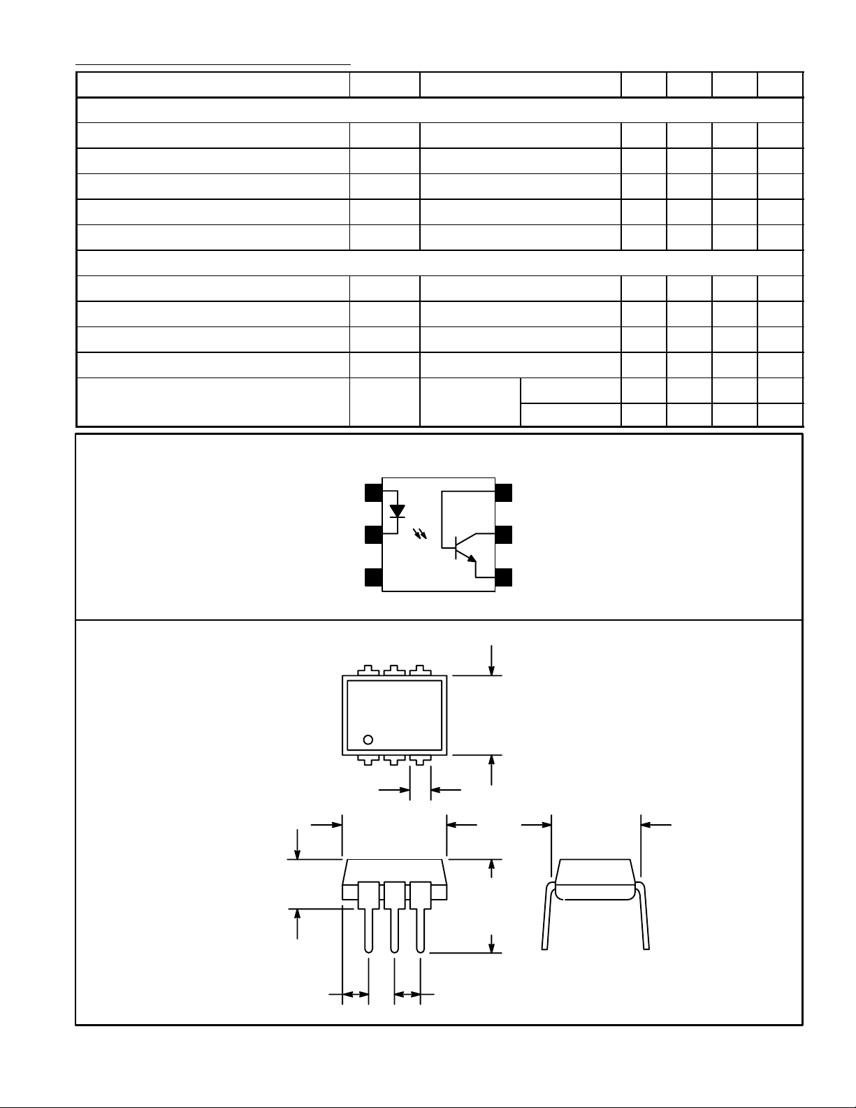
Pin Connection Diagram
Anode
Cathode
2
f
= 60mA, IC = 1.6mA 100 – – V
V
= 500V
(I–O)
V
= 0, f = 1MH
(I–O)
VCE = 10V,
RL = 100Ω
DC
Z
ICE = 2mA – 5 – µs
ICB = 50µA – 3 – µs
Base1
6
5
Collector
100 – – GΩ
– – 2 pf
.070 (1.78) Max
.200 (5.08)
Max
3N.C.
546
123
.350 (8.89)
Max
.260
(6.6)
Max
.350
(8.89)
Max
4
Emitter
.300 (7.62)
.085 (2.16) Max
.100 (2.54)
 Loading...