

NTE NTE3031 Datasheet
NTE3031
Phototransistor Detector
NPN–Si, Visible & IR
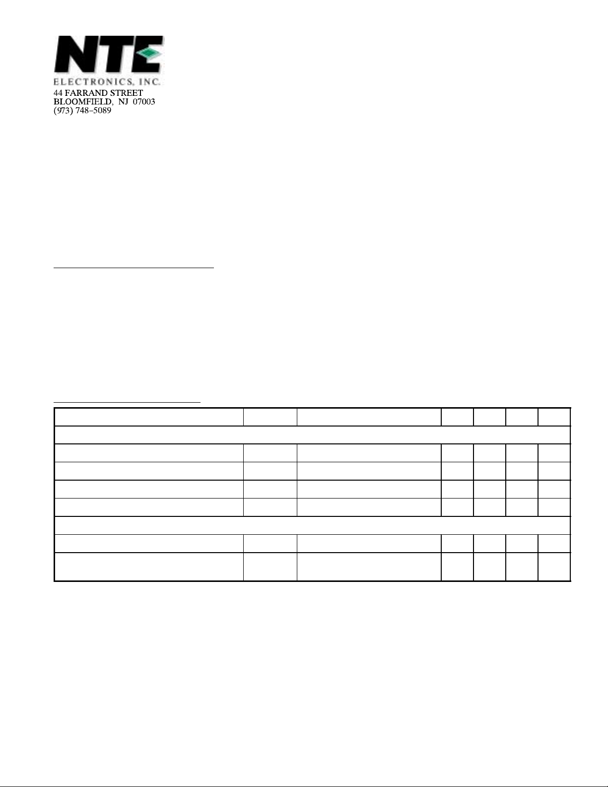
Absolute Maximum Ratings: (TA = +25°C unless otherwise specified)
Collector–Emitter Voltage, V
Emitter–Collector Voltage, V
Continuous Device Dissipation, P
Derate Above 25°C 1.43mW/°C. . . . . . . . . . . . . . . . . . . . . . . . . . . . . . . . . . . . . . . . . . . . . . . . . . . .
Operating Junction Temperature Range, T
Storage Temperature Range, T
Lead temperature (During Soldering, 3 min), T
Electrical Characteristics: (TA = +25°C unless otherwise specified)
Parameter Symbol Test Conditions Min Typ Max Unit
Static Characteristics
CEO
ECO
D
J
stg
L
30V. . . . . . . . . . . . . . . . . . . . . . . . . . . . . . . . . . . . . . . . . . . . . . . . . . . . . .
5V. . . . . . . . . . . . . . . . . . . . . . . . . . . . . . . . . . . . . . . . . . . . . . . . . . . . . . .
150mW. . . . . . . . . . . . . . . . . . . . . . . . . . . . . . . . . . . . . . . . . . . . . . . .
–55° to +125°C. . . . . . . . . . . . . . . . . . . . . . . . . . . . . . . . . .
–65° to +150°C. . . . . . . . . . . . . . . . . . . . . . . . . . . . . . . . . . . . . . . . . .
+260°C. . . . . . . . . . . . . . . . . . . . . . . . . . . . . . . . . . . . .
Collector Dark Current I
Collector–Emitter Breakdown Voltage V
Emitter–Collector Breakdown Voltage V
Saturation Voltage V
Optical Characteristics
Light Current I
Photo Current Rise Time t
(BR)CEOIC
(BR)ECOIE
CE(sat)IC
D
L
r
VCE = 10V – – 100 nA
= 100µA 30 – – V
= 100µA 5 – – V
= 0.4mA – 0.2 – V
VCE = 5V, RL = 100Ω, Note 1 1 – – mA
RL = 1000Ω, VCC = 5V,
= 1mA (Peak)
I
L
– 6 – µs
Note 1. Radiation flux density (H) equal to 5mW/cm2 emitted from a tungsten source at a color
temperature of 2875 K.
Note 2. Angular response is defined as the total included angle between the half sensitivity points
and assuming a point source.
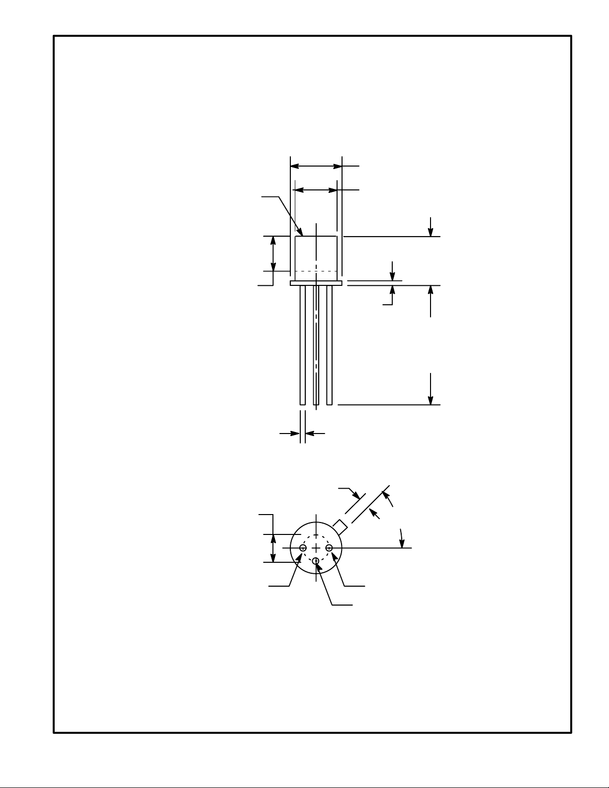
.210 (5.33) Dia
.155 (3.94) Dia
Window on
Center Line
.150 (3.81) Die
Seating Plane
.184 (4.67) Dia
.208
(5.28)
.021
(0.53)
.500
(12.7)
Min
.018 (0.45) Dia Typ
.100 (2.54) Dia
Collector Emitter
.040 (1.02)
45°
Base
 Loading...