

NTE NTE29, NTE30 Datasheet
NTE29 (NPN) & NTE30 (PNP)
Silicon Complementary Transistors
High Power, High Current Switch
Description:
The NTE29 ( NPN) a nd N TE30 ( PNP) a re c ompelmentary p ower t ransistors i n a T O3 t ype c ase d esigned
for use in high power amplifier and switching circuit applications.
Features:
D High Current Capability: IC = 50A (Continuous)
D DC Current Gain: h
D Low Collector–Emitter Saturation Voltage: V
Absolute Maximum Ratings:
Collector–Emitter Voltage, V
Collector–Base Voltage, V
Emitter–Base Voltage, V
Continuous Collector Current, I
Base Current, I
B
Total Device Dissipation (T
Derate Above 25°C 1.715W/°C. . . . . . . . . . . . . . . . . . . . . . . . . . . . . . . . . . . . . . . . . . . . . . . . . . . . .
Operating Junction Temperature Range, T
Storage Temperature Range, T
Thermal Resistance, Junction–to–Case, R
= 15 to 60 @ IC = 25A
FE
CEO
CB
EB
C
= +25°C), P
C
stg
D
J
thJC
CE(sat)
= 1V Max @ IC = 25A
80V. . . . . . . . . . . . . . . . . . . . . . . . . . . . . . . . . . . . . . . . . . . . . . . . . . . . . .
80V. . . . . . . . . . . . . . . . . . . . . . . . . . . . . . . . . . . . . . . . . . . . . . . . . . . . . . . . .
5V. . . . . . . . . . . . . . . . . . . . . . . . . . . . . . . . . . . . . . . . . . . . . . . . . . . . . . . . . . .
50A. . . . . . . . . . . . . . . . . . . . . . . . . . . . . . . . . . . . . . . . . . . . . . . . . . . . .
15A. . . . . . . . . . . . . . . . . . . . . . . . . . . . . . . . . . . . . . . . . . . . . . . . . . . . . . . . . . . . . . . . . . .
300W. . . . . . . . . . . . . . . . . . . . . . . . . . . . . . . . . . . . . . . . . . .
–65° to +200°C. . . . . . . . . . . . . . . . . . . . . . . . . . . . . . . . . .
–65° to +200°C. . . . . . . . . . . . . . . . . . . . . . . . . . . . . . . . . . . . . . . . . .
0.584°C/W. . . . . . . . . . . . . . . . . . . . . . . . . . . . . . . . . . .
Electrical Characteristics:
Parameter Symbol Test Conditions Min Typ Max Unit
OFF Characteristics
Collector–Emitter Sustaining Voltage V
Collector Cutoff Current I
Emitter Cutoff Current I
(TC = +25°C unless otherwise specified)
CEO(sus)IC
CEO
I
CEX
I
CBO
EBO
VCE = 40V, IB = 0 – – 1 mA
VCE = 80V, V
VCE = 80V, V
T
VCB = 80V, IE = 0 – – 2 mA
VBE = 5V, IC = 0 – – 5 mA
= 0.2A, IB = 0, Note 1 80 – – V
= 1.5V – – 2 mA
EB(off)
= +150°C
C
EB(off)
= 1.5V,
– – 10 mA
Electrical Characteristics (Cont’d): (TC = +25°C unless otherwise specified)
Parameter Symbol Test Conditions Min Typ Max Unit
ON Characteristics (Note 1)
DC Current Gain h
Collector–Emitter Saturation Voltage V
Base–Emitter Saturation Voltage V
Base–Emitter ON Voltage V
Dynamic Characteristics
Current Gain–Bandwidth Product f
Output Capacitance C
Small–Signal Current Gain h
CE(sat)IC
BE(sat)IC
BE(on)IC
FE
T
ob
fe
IC = 25A, VCE = 2V 15 – 60
IC = 50A, VCE = 5V 5 – –
= 25A, IB = 2.5A – – 1 V
IC = 50A, IB = 10A – – 5 V
= 25A, IB = 2.5A – – 2 V
= 25A, VCE = 2V – – 2 V
IC = 5A, VCE = 10V, f = 1MHz 2 – – MHz
VCB = 10V, IE = 0, f = 0.1MHz – – 1200 pF
IC = 10A, VCE = 5V, f = 1kHz 15 – –
Note 1. Pulse Test: Pulse Width ≤ 300µs, Duty Cycle ≤ 2%.
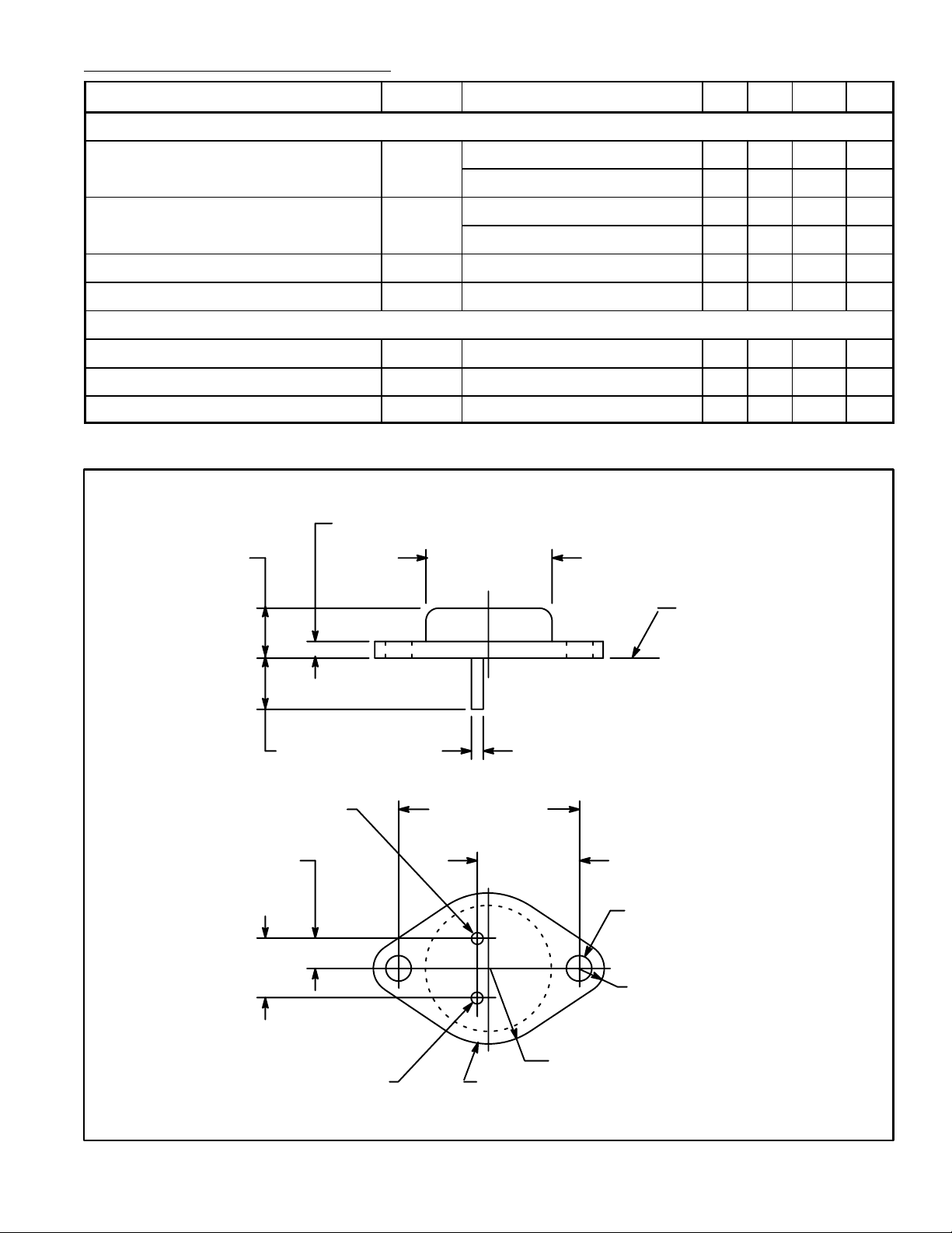
.135 (3.45) Max
.350 (8.89)
.875 (22.2)
Dia Max
.215 (5.45)
.430
(10.92)
Emitter
Seating
Plane
.040 (1.02).312 (7.93) Min
1.187 (30.16)
.665
(16.9)
.156 (3.96) Dia
(2 Holes)
.188 (4.8) R Max
.525 (13.35) R Max
Collector/CaseBase
 Loading...