

NTE NTE2987 Datasheet

NTE2987
Logic Level MOSFET
N–Channel, Enhancement Mode
High Speed Switch
Features:
D Avalanche Rugged Technology
D Logic Level Gate Drive
D R
D +175°C Operating Temperature
D Fast Switching
D Low Gate Charge
D High Current Capability
Absolute Maximum Ratings:
Drain Current, I
Total Power Dissipation (T
Gate–Source Voltage, V
Avalanche Current, Repetitive or Non–Repetitive (Note 2), I
Single Pulsed Avalanche Energy (Note 3), E
Repetitive Avalanche Energy (Note 2), E
Avalanche Current, Repetitive or Non–Repetitive (Note 4), I
Drain–Source Voltage (V
Drain–Gate Voltage (R
Operating Junction Temperature, T
Storage Temperature Range, T
Maximum Lead Temperature (During Soldering, 1.6mm from case, 10sec), T
Thermal Resistance:
Note 1. Pulse width limited by safe operating area.
Note 2. Pulse width limited by T
Note 3. V
Note 4. T
(on) = 0.09Ω Typ. at VGS = 5V
DS
D
Continuous
TC = +25°C 20A. . . . . . . . . . . . . . . . . . . . . . . . . . . . . . . . . . . . . . . . . . . . . . . . . . . . . . . . . . . . . . .
T
= +100°C 14A. . . . . . . . . . . . . . . . . . . . . . . . . . . . . . . . . . . . . . . . . . . . . . . . . . . . . . . . . . . . . .
C
Pulsed (Note 1) 80A. . . . . . . . . . . . . . . . . . . . . . . . . . . . . . . . . . . . . . . . . . . . . . . . . . . . . . . . . . . . . .
= +25°C), P
C
D
Derate Above 25°C 0.7W/°C. . . . . . . . . . . . . . . . . . . . . . . . . . . . . . . . . . . . . . . . . . . . . . . . . . . . . . .
GS
AR
AS
AR
AR
= 0), V
GS
= 20kΩ), V
GS
Maximum Junction–to–Case, R
DS
DGR
J
stg
thJC
Typical Case–to–Sink (Mounting surface flat, smooth, and greased), R
Maximum Junction–to–Ambient (Free Air Operation), R
max, Duty Cycle < 1%.
J
= 25V, ID = IAR, Starting TJ = +175°C.
DD
= +100°C, Pulse width limited by TJ max, Duty Cycle < 1%.
C
thJA
L
thCS
105W. . . . . . . . . . . . . . . . . . . . . . . . . . . . . . . . . . . . . . . . . . .
±15V. . . . . . . . . . . . . . . . . . . . . . . . . . . . . . . . . . . . . . . . . . . . . . . . . . . . . . . . .
20A. . . . . . . . . . . . . . . . . . . . . . . . . . .
120mJ. . . . . . . . . . . . . . . . . . . . . . . . . . . . . . . . . . . . . .
30mJ. . . . . . . . . . . . . . . . . . . . . . . . . . . . . . . . . . . . . . . . . .
14A. . . . . . . . . . . . . . . . . . . . . . . . . . .
100V. . . . . . . . . . . . . . . . . . . . . . . . . . . . . . . . . . . . . . . . . . . . . . . .
100V. . . . . . . . . . . . . . . . . . . . . . . . . . . . . . . . . . . . . . . . . . . . .
+175°C. . . . . . . . . . . . . . . . . . . . . . . . . . . . . . . . . . . . . . . . . . . . . . .
–65° to +175°C. . . . . . . . . . . . . . . . . . . . . . . . . . . . . . . . . . . . . . . . . .
+300°C. . . . . . . . . .
1.43°C/W. . . . . . . . . . . . . . . . . . . . . . . . . . . . . . . . . . . . . . . .
0.5°C/W. . . . . .
62.5°C/W. . . . . . . . . . . . . . . . . . .
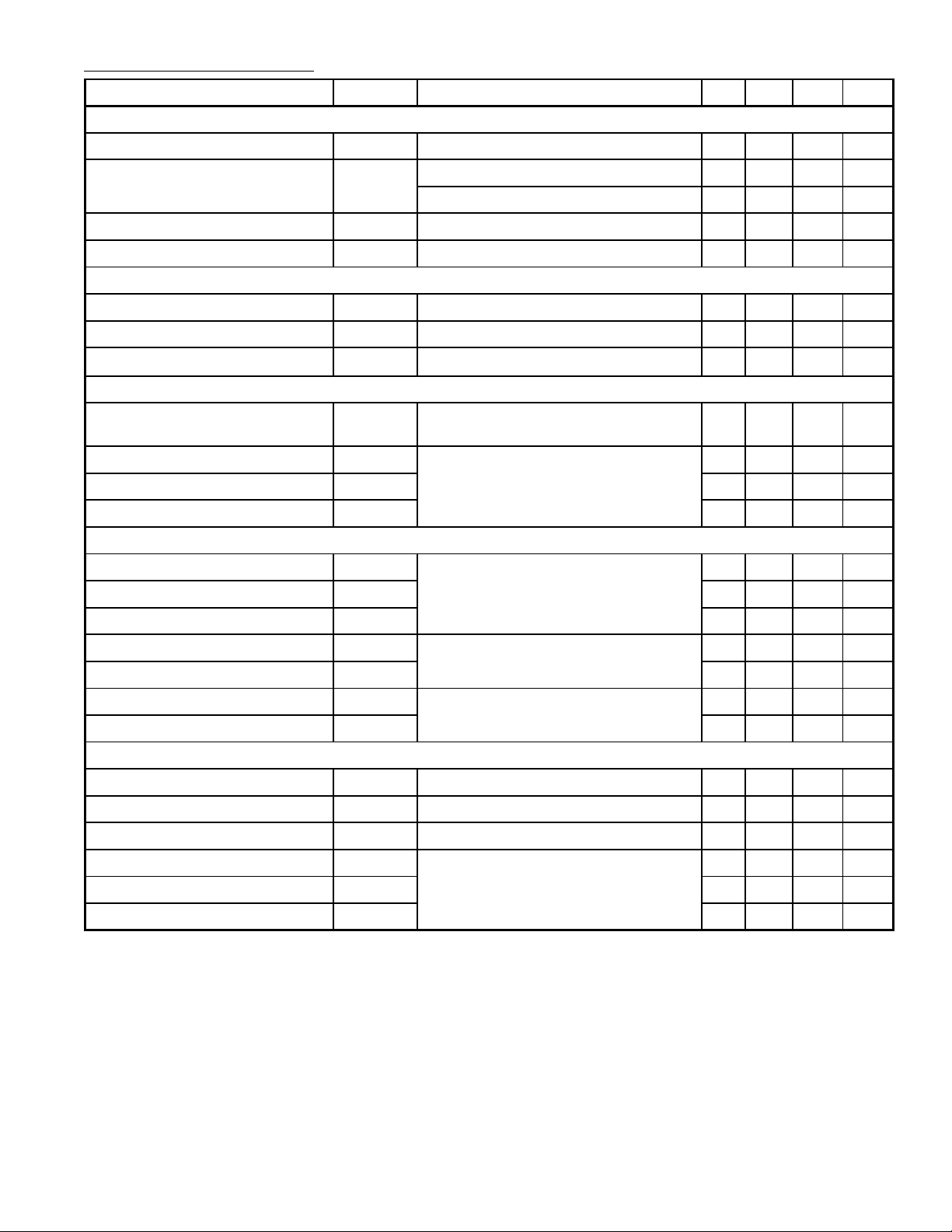
Electrical Characteristics: (TC = +25°C unless otherwise specified)
Parameter Symbol Test Conditions Min Typ Max Unit
OFF
Drain–Source Breakdown Voltage BV
Drain–to–Source Leakage Current I
DSS
DSS
VGS = 0v, ID = 250µA 100 – – V
VDS = 100V, VGS = 0 – – 1 µA
VDS = 80V, VGS = 0V, , TC = +150°C – – 10 µA
Gate–Source Leakage Forward I
Gate–Source Leakage Reverse I
GSS
GSS
VGS = 15V – – 100 nA
VGS = –15V – – –100 nA
ON (Note 5)
Gate Threshold Voltage V
Static Drain–Source ON Resistance R
On–State Drain Current
GS(th)
DS(on)
I
D(on)
VDS = VGS, ID = 250µA 1.0 1.6 2.5 V
VGS = 5V, ID = 10A – 0.09 0.12 Ω
VDS > I
Dynamic
Forward Transconductance g
fs
VDS > I
Note 5
Input Capacitance C
Output Capacitance C
Reverse Transfer Capacitance C
iss
oss
rss
VGS = 0V, VDS = 25V, f = 1MHz – 1200 1500 pF
Switching
Total Gate Charge Q
Gate–Source Charge Q
Gate–Drain (“Miller”) Charge Q
Turn–On Delay Time t
d(on)
Rise Time t
Turn–Off Delay Time t
d(off)
Fall Time t
gs
gd
r
f
VGS = 5V, ID = 20A, VDD = 80V
g
VDD = 30V
VGS = 5V
VDD = 80V
VGS = 5V
Source–Drain Diode Ratings and Characteristics
x R
D(on)
D(on)
DS(on)
x R
DS(on)
ID = 10A, RG = 50Ω,
,
ID = 20A, RG = 50Ω,
,
max, VGS = 10V
max, ID = 10A,
20 – – A
10 16 – mhos
– 250 350 pF
– 60 90 pF
– 22 30 nC
– 6 – nC
– 12 – nC
– 50 70 ns
– 140 200 ns
– 80 110 ns
– 80 110 ns
Continuous Source Current I
Pulse Source Current I
Diode Forward Voltage V
Reverse Recovery Time t
Reverse Recovery Charge Q
Reverse Recovery Current
I
RRM
S
SM
SD
rr
(Body Diode) – – 20 A
(Body Diode) Note 1 – – 80 A
ISD = 20A, VGS = 0V, Note 5 – – 1.5 V
TJ = +150°C, VDD = 50V, ISD = 20A,
di/dt = 100A/µs
rr
Note 1. Pulse width limited by safe operating area.
Note 5. Pulse Test: Pulse Width = 300µs, Duty Cycle = 1.5%.
– 130 – ns
– 0.4 – µC
– 6 – A
 Loading...