

NTE NTE2974 Datasheet
NTE2974
MOSFET
N–Channel, Enhancement Mode
High Speed Switch
Features:
D Low On–State Resistance: R
D Low Input Capacitance: C
= 1150pF Typ
iss
D High Avalanche Capability Ratings
D Isolated TO220 Type Package
Absolute Maximum Ratings: (TA = +25°C unless otherwise specified)
Drain–to–Source Voltage, V
Gate–to–Source Voltage, V
Drain Current, I
D
DSS
GSS
DC ±6.0A. . . . . . . . . . . . . . . . . . . . . . . . . . . . . . . . . . . . . . . . . . . . . . . . . . . . . . . . . . . . . . . . . . . . . . .
Pulse (Note 1) ±24A. . . . . . . . . . . . . . . . . . . . . . . . . . . . . . . . . . . . . . . . . . . . . . . . . . . . . . . . . . . . . .
Total Power Dissipation, P
T
TC = +25°C 35W. . . . . . . . . . . . . . . . . . . . . . . . . . . . . . . . . . . . . . . . . . . . . . . . . . . . . . . . . . . . . . . . .
TA = +25°C 2.0W. . . . . . . . . . . . . . . . . . . . . . . . . . . . . . . . . . . . . . . . . . . . . . . . . . . . . . . . . . . . . . . . .
Single Avalanche Current (Note 2), I
Single Avalanche Energy (Note 2), E
Channel Temperature, T
Storage Temperature Range, T
ch
stg
DS(on)
AS
AS
= 1.1Ω Max (VGS = 10V, ID = 3A)
600V. . . . . . . . . . . . . . . . . . . . . . . . . . . . . . . . . . . . . . . . . . . . . . . . . . . . .
±30V. . . . . . . . . . . . . . . . . . . . . . . . . . . . . . . . . . . . . . . . . . . . . . . . . . . . .
6.0A. . . . . . . . . . . . . . . . . . . . . . . . . . . . . . . . . . . . . . . . . . . . . . .
12mJ. . . . . . . . . . . . . . . . . . . . . . . . . . . . . . . . . . . . . . . . . . . . . .
+150°C. . . . . . . . . . . . . . . . . . . . . . . . . . . . . . . . . . . . . . . . . . . . . . . . . . . . . . . .
–55° to +150°C. . . . . . . . . . . . . . . . . . . . . . . . . . . . . . . . . . . . . . . . . .
Note 1. PW ≤ 10µs, Duty Cycle ≤ 1%.
Note 2. Starting Tch = +25°C, RG = 25Ω, VGS = 20V → 0.
Electrical Characteristics: (TA = +25°C unless otherwise specified)
Parameter Symbol Test Conditions Min Typ Max Unit
Drain–to–Source On–State Resistance R
Gate–to–Source Cutoff Voltage V
Forward Transfer Admittance |yfs| VDS = 10V, ID = 3A 2.0 – – S
Drain Leakage Current I
Gate–to–Source Leakage Current I
DS(on)VGS
GS(off)VDS
DSS
GSS
= 10V, ID = 3A – 0.8 1.1 Ω
= 10V, ID = 1mA 2.5 – 3.5 V
VDS = 600V, VGS = 0 – – 100 µA
VGS = ±30V, VDS = 0 – – ±100 nA
Electrical Characteristics (Cont’d): (TA = +25°C unless otherwise specified)
Parameter Symbol Test Conditions Min Typ Max Unit
Input Capacitance C
Output Capacitance C
Reverse Transfer Capacitance C
Turn–On Delay Time t
Rise Time t
Turn–Off Delay Time t
Fall Time t
Total Gate Charge Q
Gate–to–Source Charge Q
Gate–to–Drain Charge Q
Diode Forward Voltage V
Reverse Recovery Time t
Reverse Recovery Charge Q
d(on)
d(off)
F(S–D)IF
iss
oss
rss
r
f
G
GS
GD
rr
rr
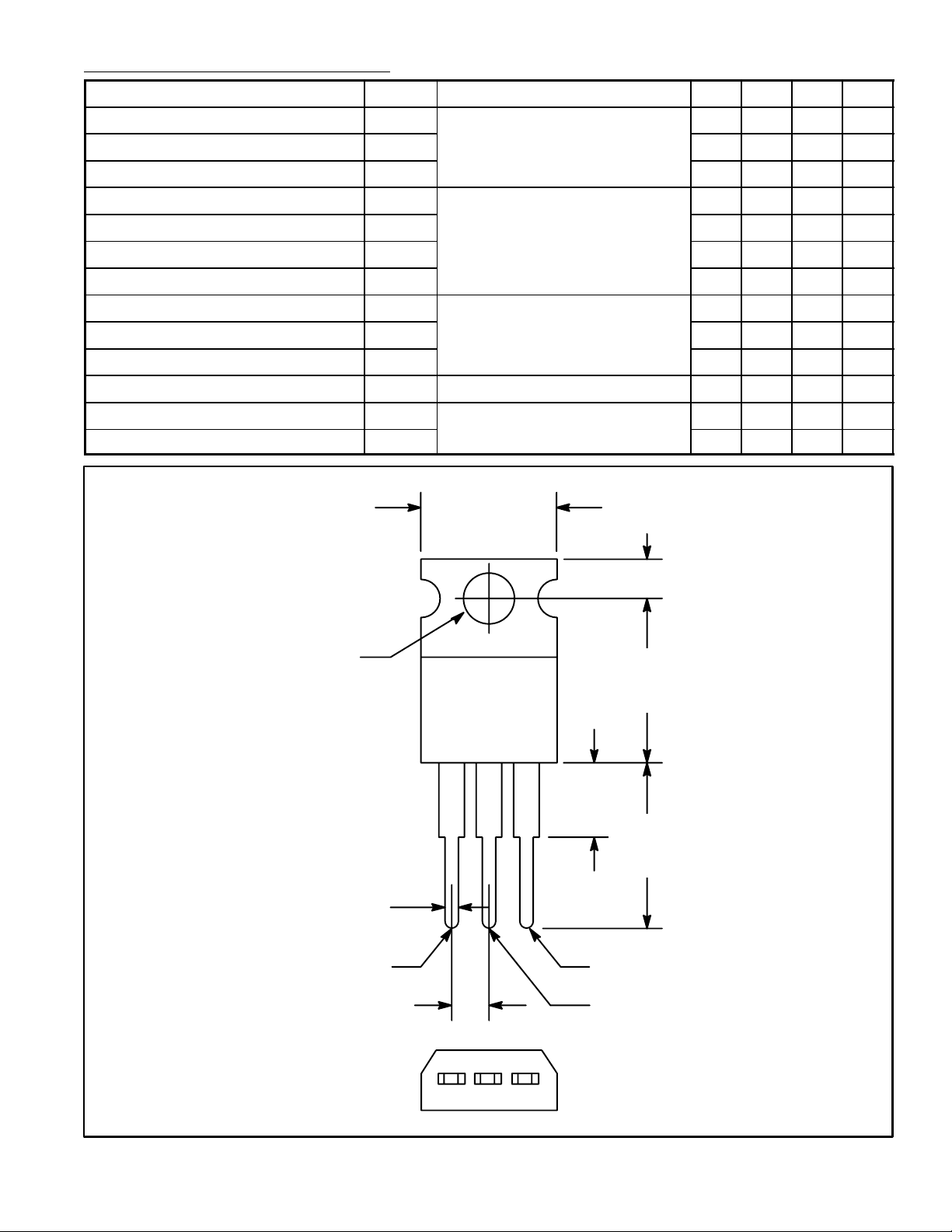
.420 (10.67)
VDS = 10V, VGS = 0, f = 1MHz
VGS = 10V, VDD = 150V, ID = 3A,
RG = 10Ω, RL = 37.5Ω
VGS = 10V, ID = 6A, VDD = 480V
= 6A, VGS = 0 – 1.0 – V
IF = 6A, di/dt = 50A/µs
– 1150 – pF
– 260 – pF
– 60 – pF
– 15 – ns
– 15 – ns
– 75 – ns
– 13 – ns
– 40 – nC
– 6 – nC
– 20 – nC
– 370 – ns
– 1.5 – µC
Max
.147 (3.75)
Dia Max
.070 (1.78) Max
Gate
.100 (2.54)
.110 (2.79)
Isol
.500
(12.7)
Max
.250 (6.35)
Max
.500
(12.7)
Min
Source
Drain
 Loading...