

NTE NTE2972 Datasheet
NTE2972
MOSFET
N–Channel, Enhancement Mode
High Speed Switch
Applications:
D SMPS
D DC–DC Converter
D Battery Charger
D Power Supply of Printer
D Copier
D HDD, FDD, TV, VCR
D Personal Computer
Absolute Maximum Ratings: (TC = +25°C unless otherwise specified)
Drain–Source Voltage (VGS = 0V), V
Gate–Source Voltage (VDS = 0V), V
Drain Current, I
D
Continuous 10A. . . . . . . . . . . . . . . . . . . . . . . . . . . . . . . . . . . . . . . . . . . . . . . . . . . . . . . . . . . . . . . . . .
Pulsed 30A. . . . . . . . . . . . . . . . . . . . . . . . . . . . . . . . . . . . . . . . . . . . . . . . . . . . . . . . . . . . . . . . . . . . . .
Maximum Power Dissipation, P
Channel Temperature Range, T
Storage Temperature Range, T
Thermal Resistance, Channel–to–Case, R
DSS
GS
D
ch
stg
th(ch–c)
700V. . . . . . . . . . . . . . . . . . . . . . . . . . . . . . . . . . . . . . . . . . . . . .
±30V. . . . . . . . . . . . . . . . . . . . . . . . . . . . . . . . . . . . . . . . . . . . . . .
150W. . . . . . . . . . . . . . . . . . . . . . . . . . . . . . . . . . . . . . . . . . . . . . . . . . .
–55° to +150°C. . . . . . . . . . . . . . . . . . . . . . . . . . . . . . . . . . . . . . . . . .
–55° to +150°C. . . . . . . . . . . . . . . . . . . . . . . . . . . . . . . . . . . . . . . . . .
0.83°C/W. . . . . . . . . . . . . . . . . . . . . . . . . . . . . . . . . .
Electrical Characteristics: (Tch = +25°C unless otherwise specified)
Parameter Symbol Test Conditions Min Typ Max Unit
Drain–Source Breakdown Voltage V
Gate–Source Breakdown Voltage V
Gate–Source Leakage I
Zero Gate Voltage Drain Current I
Gate Threshold Voltage V
Static Drain–Source ON Resistance R
Drain–Source On–State Voltage V
Forward Transfer Admittance |yfs| VGS = 10V, ID = 5A 4.8 8.0 – S
(BR)DSSVDS
(BR)GSSVDS
GSS
DSS
GS(th)
DS(on)VGS
DS(on)VGS
= 0V, ID = 1mA 700 – – V
= 0V, IG = ±100µA ±30 – – V
VGS = ±25V, VDS = 0V – – ±10 µA
VDS = 700V, VGS = 0 – – 1.0 mA
VDS = 10V, ID = 1mA 2.0 3.0 4.0 V
= 10V, ID = 5A – 1.0 1.3 Ω
= 10V, ID = 5A – 5.0 6.5 V
Electrical Characteristics (Cont’d): (Tch = +25°C unless otherwise specified)
Parameter Symbol Test Conditions Min Typ Max Unit
Input Capacitance C
Output Capacitance C
Reverse Transfer Capacitance C
Turn–On Delay Time t
Rise Time t
Turn–Off Delay Time t
Fall Time t
Diode Forward Voltage V
d(on)
d(off)
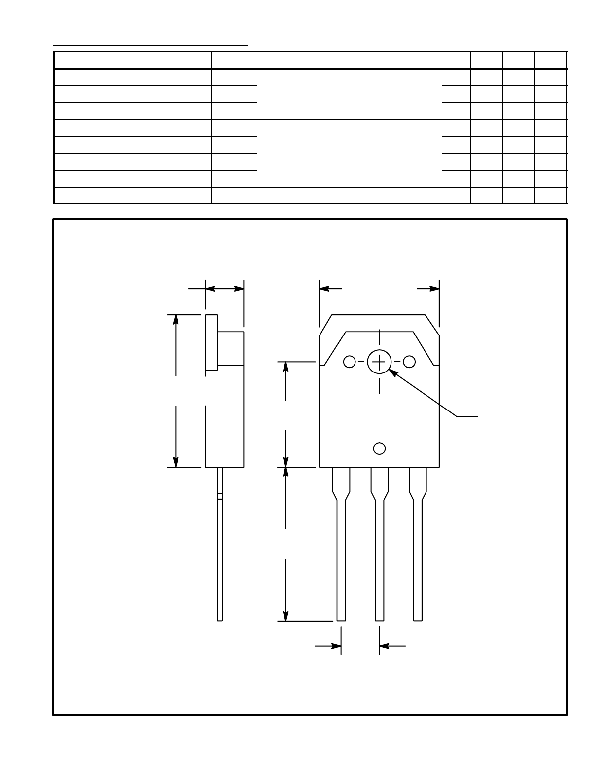
.190 (4.82)
iss
oss
rss
r
f
SD
VGS = 0V, VDS = 25V, f = 1MHz – 1380 – pF
– 150 – pF
– 32 – pF
VDD = 200V
R
= RGS = 50Ω
GEN
IS = 5A, VGS = 0V – 1.5 2.0 V
= 5A, VGS = 10V,
, ID
– 25 – ns
– 33 – ns
– 170 – ns
– 55 – ns
.615 (15.62)
.787
(20.0)
.591
(15.02)
.787
(20.0)
.126 (3.22) Dia
GDS
.215 (5.47)
 Loading...