

NTE NTE2920 Datasheet

NTE2920
MOSFET
N–Ch, Enhancement Mode
High Speed Switch
Features:
D Dynamic dv/dt Rating
D Isolated Central Mounting Hole
D Fast Switching
D +175°C Operating Temperature
D Ease of Paralleling
D Simple Drive Requirements
Absolute Maximum Ratings:
Continuous Drain Current (VGS = 10V), I
TC = +25°C (Note 5) 70A. . . . . . . . . . . . . . . . . . . . . . . . . . . . . . . . . . . . . . . . . . . . . . . . . . . . . . . . . .
= +100°C 64A. . . . . . . . . . . . . . . . . . . . . . . . . . . . . . . . . . . . . . . . . . . . . . . . . . . . . . . . . . . . . . . . .
T
C
Pulsed Drain Current (Note 1), I
Power Dissipation (T
= +25°C), P
C
DM
D
Derate Linearly Above 25°C 1.5W/°C. . . . . . . . . . . . . . . . . . . . . . . . . . . . . . . . . . . . . . . . . . . . . . .
Gate–to–Source Voltage, V
GS
Single Pulse Avalanche Energy (Note 2), E
Peak Diode Recovery dv/dt (Note 3), dv/dt 4.5V/ns. . . . . . . . . . . . . . . . . . . . . . . . . . . . . . . . . . . . . . . . .
Operating Junction Temperature Range, T
Storage Temperature Range, T
stg
Lead Temperature (During Soldering, 1.6mm from case for 10sec), T
Mounting Torque (6–32 or M3 Screw) 10 lbfin (1.1Nm). . . . . . . . . . . . . . . . . . . . . . . . . . . . . . . . . . . .
Thermal Resistance, Junction–to–Case, R
Thermal Resistance, Junction–to–Ambient, R
Typical Thermal Resistance, Case–to–Sink (Flat, Greased Surface), R
D
AS
J
thJC
thJA
L
thCS
–55° to +175°C. . . . . . . . . . . . . . . . . . . . . . . . . . . . . . . . . .
–55° to +175°C. . . . . . . . . . . . . . . . . . . . . . . . . . . . . . . . . . . . . . . . . .
0.65°C/W. . . . . . . . . . . . . . . . . . . . . . . . . . . . . . . . . . . .
0.24°C/W. . . . . . . . . . .
360A. . . . . . . . . . . . . . . . . . . . . . . . . . . . . . . . . . . . . . . . . . . . . . . . . .
230W. . . . . . . . . . . . . . . . . . . . . . . . . . . . . . . . . . . . . . . . . . . . . . . .
±20. . . . . . . . . . . . . . . . . . . . . . . . . . . . . . . . . . . . . . . . . . . . . . . . . . . . . . .
640mJ. . . . . . . . . . . . . . . . . . . . . . . . . . . . . . . . . . . . . . .
+300°C. . . . . . . . . . . . . . . . .
40°C/W. . . . . . . . . . . . . . . . . . . . . . . . . . . . . . . . . . .
Note 1. Repetitive rating; pulse width limited by maximum junction temperature.
Note 2. V
Note 3. I
= 25V, starting TJ = +25°C, L = 92µH, RG = 25Ω, IAS = 90A
DD
≤ 90A, di/dt ≤ 200A/µs, VDD ≤ 60V, TJ ≤ +175°C
SD
Note 4. Pules Width ≤ 300µs, Duty Cycle ≤ 2%.
Note 5. Current limited by the package, (Die Current = 90A).
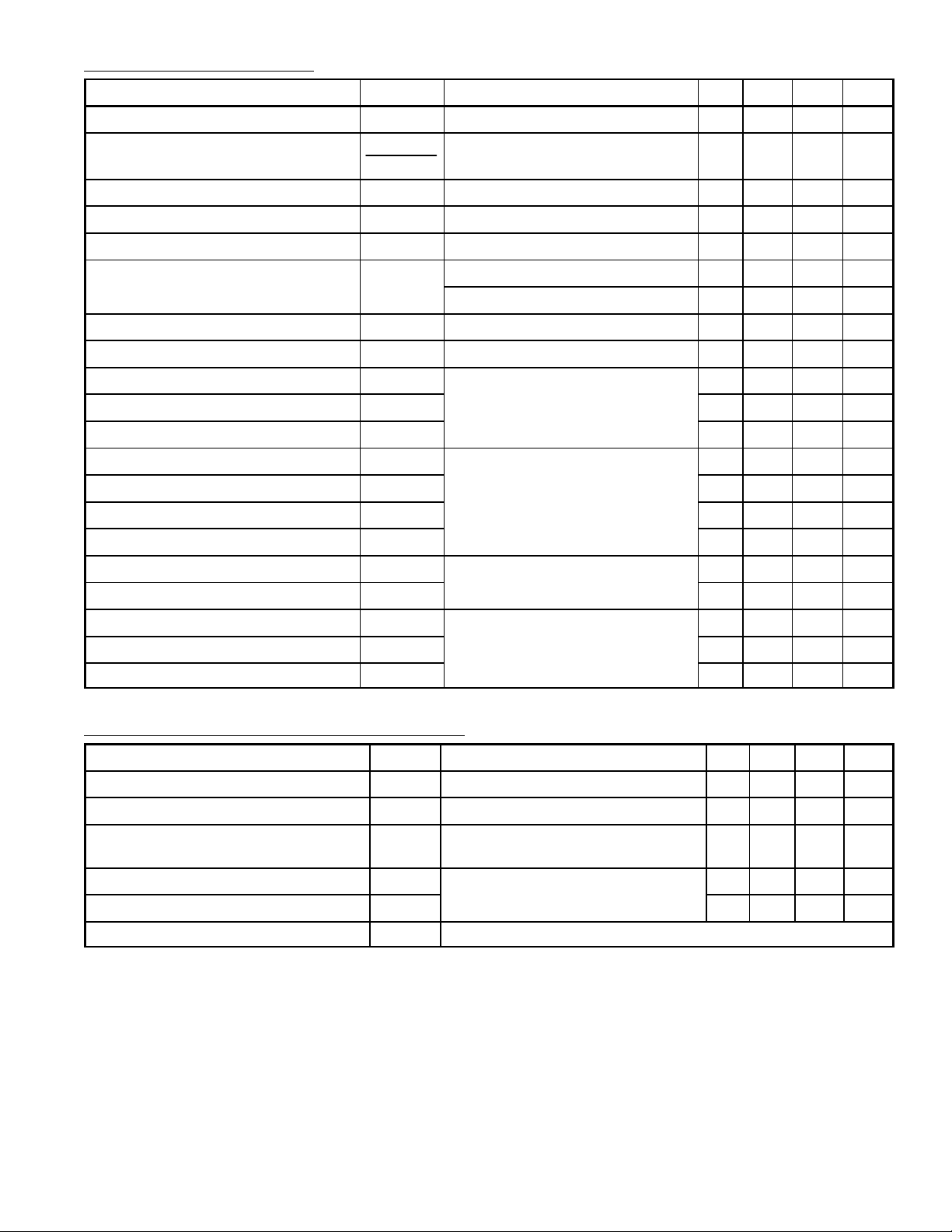
Electrical Characteristics: (TJ = +25°C unless otherwise specified)
Parameter Symbol Test Conditions Min Typ Max Unit
Drain–to–Source Breakdown Voltage V
Breakdown Voltage Temp. Coefficient ∆V
(BR)DSSVGS
(BR)DSS
∆T
Static Drain–to–Source On–Resistance R
Gate Threshold Voltage V
DS(on)
GS(th)
Forward Transconductance g
Drain–to–Source Leakage Current I
Gate–to–Source Forward Leakage I
Gate–to–Source Reverse Leakage I
DSS
GSS
GSS
Total Gate Charge Q
Gate–to–Source Charge Q
Gate–to–Drain (“Miller”) Charge Q
Turn–On Delay Time t
d(on)
Rise Time t
Turn–Off Delay Time t
d(off)
Fall Time t
Internal Drain Inductance L
Internal Source Inductance L
Input Capacitance C
Output Capacitance C
Reverse Transfer Capaticance C
fs
gs
gd
r
f
D
S
iss
oss
rss
= 0V, ID = 250µA 60 – – V
Reference to +25°C, ID = 1mA – 0.056 – V/°C
J
VGS = 10V, ID = 54A, Note 4 – – 0.014 Ω
VDS = VGS, ID = 250µA 2.0 – 4.0 V
VDS = 25V, ID = 54A, Note4 25 – – mhos
VDS = 60V, VGS = 0V – – 25 µA
VDS = 48V, VGS = 0V, TJ = +150°C – – 250 µA
VGS = 20V – – 100 nA
VGS = –20V – – –100 nA
ID = 64A, VDS = 48V, VGS = 10V,
g
Note 4
– – 160 nC
– – 48 nC
– – 54 nC
VDD = 30V, ID = 64A, RG = 6.2Ω,
RD = 0.45Ω, Note 4
– 20 – ns
– 160 – ns
– 83 – ns
– 150 – ns
Between lead, .250in. (6.0) m m from
package and center of die contact
VGS = 0V, VDS = 25V, f = 1MHz
– 5.0 – nH
– 13 – nH
– 4500 – pF
– 2000 – pF
– 300 – pF
Source–Drain Ratings and Characteristics:
Parameter Symbol Test Conditions Min Typ Max Unit
Continuous Source Current (Body Diode) I
Pulsed Source Current (Body Diode) I
Diode Forward Voltage V
SM
Note 5 – – 70 A
S
Note 1 – – 360 A
TJ = +25°C, IS = 90A, VGS = 0V,
SD
– – 2.5 V
Note 4
Reverse Recovery Time t
Reverse Recovery Charge Q
Forward Turn–On Time t
TJ = +25°C, IF = 64A,
rr
di/dt = 100A/µs, Note 4
rr
Intrinsic turn–on time is neglegible (turn–on is dominated by LS+LD)
on
– 270 540 ns
– 1.1 2.2 µC
Note 1. Repetitive rating; pulse width limited by maximum junction temperature.
Note 4. Pulse width ≤ 300µs; duty cycle ≤ 2%.
Note 5. Current limited by the package, (Die Current = 90A).
 Loading...