

NTE NTE2764 Datasheet

NTE2764
Integrated Circuit
NMOS, 64K Erasable EPROM, 200ns
Description:
The NTE2764 is a 65,536–bit (8192 X 8 bit) Ultraviolet Erasable and Electrically Programmable
Read–Only Memory (EPROM) in a 28–Lead DIP type package which operates from a single +5V supply, making it ideal for microprocessor applications. It features an output enable control and offers
a standby mode with an attendant 67% savings in power consumption.
A distinctive feature of the NTE2764 is a separate output control, output enable (OE) from the chip
enable control (CE). The OE control eliminates bus contention in multiple–bus microprocessor systems. The NTE2764 features fast, simple one–pulse programming controlled by TTL–level signals.
Total programming time for all 65,536 bits is 420 seconds.
Features:
D Ultraviolet Erasable and Electrically Programmable
D Access Time: 250ns Max
D Single Location Programming
D Programmable with Single Pulse
D Low Power Dissipation: 150mA Max (Active Current)
50mA Max (Standby Current)
D Input/Output TTL Compatible for Reading and Programming
D Single +5V Power Supply
D Three–State Outputs
Absolute Maximum Ratings: (TA = +25°C, Note 1 unless otherwise specified)
Supply Voltage, V
Supply Voltage, V
Output Voltage, V
Input Voltage, V
CC
PP
OUT
IN
Operating Temperature Range, T
Storage Temperature Range, T
stg
opr
–0.6 to +6V. . . . . . . . . . . . . . . . . . . . . . . . . . . . . . . . . . . . . . . . . . . . . . . . . . . . . . . . .
–0.6 to +22V. . . . . . . . . . . . . . . . . . . . . . . . . . . . . . . . . . . . . . . . . . . . . . . . . . . . . . . .
–0.6 to +6V. . . . . . . . . . . . . . . . . . . . . . . . . . . . . . . . . . . . . . . . . . . . . . . . . . . . . . . .
–0.6 to +6V. . . . . . . . . . . . . . . . . . . . . . . . . . . . . . . . . . . . . . . . . . . . . . . . . . . . . . . . . . .
–10°C to +80°C. . . . . . . . . . . . . . . . . . . . . . . . . . . . . . . . . . . . . . .
–65°C to +125°C. . . . . . . . . . . . . . . . . . . . . . . . . . . . . . . . . . . . . . . .
Note 1. Exposing the device to stresses above those listed in Absolute Maximum Ratings could
cause permanent damage. The device is not meant to be operated under conditions outside
the limits described in the operational sections of this specification. Exposure to absolute
maximum rating conditions for extended periods may affect device reliability.
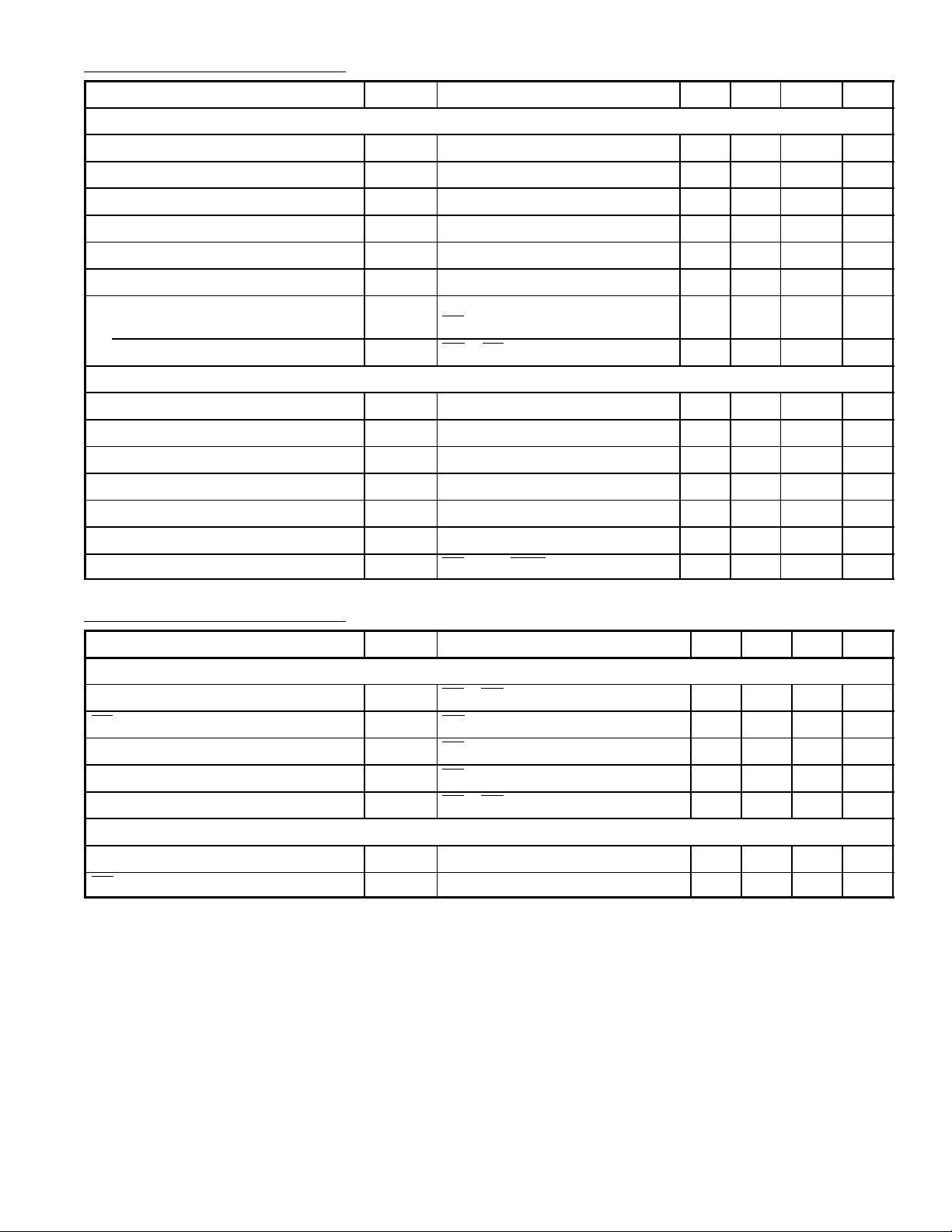
DC Electrical Characteristics: (VCC = +5V ±5% unless otherwise specified)
Parameter Symbol Test Conditions Min Typ Max Unit
Read Mode and Standby Mode (TA = 0° to +70°C)
Output High Voltage V
Output Low Voltage V
Input High Voltage V
Input Low Voltage V
Output Leakage Current I
Input Leakage Current I
LO
IOH = –400µA 2.4 – – V
OH
IOL = 2.1mA – – 0.45 V
OL
IH
IL
V
= 5.25V – – 10 µA
OUT
VIN = 5.25V – – 10 µA
LI
2.0 – VCC +1 V
–0.1 – +0.8 V
VCC Current
Standby I
Active I
CC1
CC2
CE = V
IH
OE = CE = V
– – 50 mA
IL
– – 150 mA
Program, Program Verify, and Program Inhibit Mode (TA = +25° ±5°C, VPP = +21V ±0.5V)
Input High Voltage V
Input Low Voltage V
Input Leakage Current I
Output High Voltage V
Output Low Voltage V
VCC Current I
VPP Current I
IH
LI
OH
OL
CC
PP
IL
VIN = VIL or V
IN
IOH = –400µA 2.4 – – V
IOL = 2.1mA – – 0.45 V
CE = VIL, PGM
IL – – 30 mA
= V
2.0 – VCC +1 V
–0.1 – +0.8 V
– – 10 µA
– – 150 mA
AC Electrical Characteristics: (VCC = +5V ±5% unless otherwise specified)
Parameter Symbol Test Conditions Min Typ Max Unit
Read Mode and Standby Mode (TA = 0° to +70°C, Note 2)
Address to Output Delay t
CE to Output Delay t
Output Enable to Output Delay t
Output Enable High to Output Float t
Address to Output Hold t
ACC
CE
OE
DF
OH
CE = OE = V
OE = V
CE = V
CE = V
IL
IL
IL
CE = OE = V
IL
– – 250 ns
– – 250 ns
10 – 100 ns
0 – 90 ns
IL
0 – – ns
Read Mode and Standby Mode (TA = +25°C ±5°C, VPP = +21V ±5V, Note 3)
Address Setup Time t
OE Setup Time t
AS
OES
2 – – µs
2 – – µs
Note 2. Test Conditions:
Output Load: 1 TTL gate and CL = 100pF
Input Rise and fall Times: 20ns
Input Pulse Levels: 0.8V to 2.2V
Timing Measurement Reference Level:
Inputs: 1.0V and 2.0V
Outputs: 0.8V and 2.0V
Note 3. Test Conditions:
Input Pulse Levels: 0.8V to 2.2V
Input Timing Reference Level: 1.0V and 2.0V
Output Timing Reference Level: 0.8V and 2.0V
Input Rise and fall Times: 20ns
 Loading...