

NTE NTE266 Datasheet

NTE266
Silicon NPN Transistor
Darlington Power Amplifier
Features:
D Forward Current Transfer Ratio: hFE = 40,000 Min
D Power Dissipation: 1.33W Free–Air @ T
D Hard Solder Mountdown
Applications:
D Driver, IC Driver
D Regulator
D Touch Switch
D Audio Output
D Relay Substitute
D Oscillator
D Servo–Amplifier
D Capacitor Multiplier
= +50°C
A
Absolute Maximum Ratings:
Collector–to–Emitter Voltage, V
Collector–to–Emitter Voltage, V
Emitter–to–Base Voltage, V
Collector Current, I
C
(TA = +25°C unless otherwise specified)
CEO
CES
EBO
Continuous 0.5A. . . . . . . . . . . . . . . . . . . . . . . . . . . . . . . . . . . . . . . . . . . . . . . . . . . . . . . . . . . . . . . . .
Peak 1.0A. . . . . . . . . . . . . . . . . . . . . . . . . . . . . . . . . . . . . . . . . . . . . . . . . . . . . . . . . . . . . . . . . . . . . .
Power Dissipation (T
T
= +50°C With Tab 1.33W. . . . . . . . . . . . . . . . . . . . . . . . . . . . . . . . . . . . . . . . . . . . . . . . . . . . . . . .
A
Thermal Resistance, Junction–to–Case (Note 1), R
Thermal Resistance, Junction–to–Ambient (Note 1), R
Operating Junction Temperature Range (Note 1), T
Storage Temperature range (Note 1), T
Lead Temperature (During Soldering, 1/16” from case, 10sec Max), T
= +25°C), P
C
D
thJC
thJA
J
stg
L
Note 1. Tab temperature is measured on center of tab, 1/16” from plastic body.
50V. . . . . . . . . . . . . . . . . . . . . . . . . . . . . . . . . . . . . . . . . . . . . . . . . . .
50V. . . . . . . . . . . . . . . . . . . . . . . . . . . . . . . . . . . . . . . . . . . . . . . . . . .
13V. . . . . . . . . . . . . . . . . . . . . . . . . . . . . . . . . . . . . . . . . . . . . . . . . . . . . .
6.25W. . . . . . . . . . . . . . . . . . . . . . . . . . . . . . . . . . . . . . . . . . . . . . . .
20°C/W. . . . . . . . . . . . . . . . . . . . . . . . . . . . .
75°C/W. . . . . . . . . . . . . . . . . . . . . . . . . . .
–55° to +150°C. . . . . . . . . . . . . . . . . . . . . . . . . .
–55° to +150°C. . . . . . . . . . . . . . . . . . . . . . . . . . . . . . . . . . .
+260°C. . . . . . . . . . . . . . . . .
Electrical Characteristics: (TA = +25°C unless otherwise specified)
Parameter Symbol Test Conditions Min Typ Max Unit
Forward Current Transfer Ratio h
Collector Saturation Voltage V
Base Saturation Voltage V
CE(sat)IC
BE(sat)IC
Collector Cutoff Current I
I
Emitter Cutoff Current I
Input Impedance h
Collector Capacitance C
Gain Bandwidth Product f
FE
h
CES
CBO
EBO
cbo
IC = 200mA, VCE = 5V 40k – –
IC = 20mA, VCE = 5V, f = 1kHz – 20k –
fe
= 500mA, IB = 0.5mA, Note 2 – – 1.5 V
= 500mA, IB = 0.5mA, Note 2 – – 2.0 V
VCE = 50V, TJ = +25°C – – 0.5 µA
VCE = 50V, TJ = +150°C – – 20 µA
VEB = 13V – – 0.1 µA
IC = 20mA, VCE = 5V, f = 1kHz 50 500 – Ω
ie
VCB = 10V, f = 1MHz – 5 10 pF
VCE = 5V, IC = 20mA – 75 – MHz
T
Delay Time and Rise Time td + trIC = 1A, IB1 = 1mA – 100 – ns
Storage Time t
Fall Time t
IC = 1A, IB1 = IB2 = 1mA – 350 – ns
s
IC = 1A, IB1 = IB2 = 1mA – 800 – ns
f
Note 2. Pulsed measurement: Pulse Width = 300µs, Duty Cycle ≤ 2%.
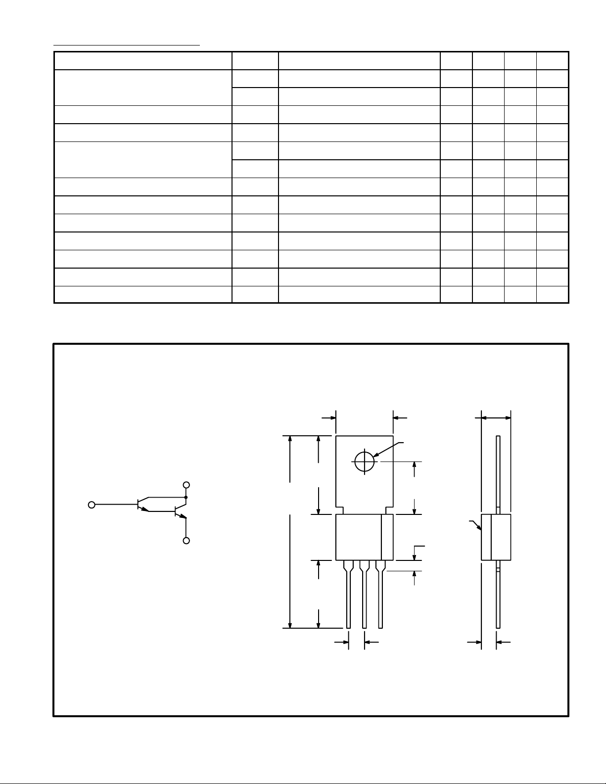
.180 (4.57).380 (9.56)
C
.500
C
B
(30.48)
E
(12.7)
1.200
Ref
.300
(7.62)
.400
(10.16)
Min
EBC
.100 (2.54) .100 (2.54)
.132 (3.35) Dia
.325
(9.52)
.070 (1.78) x 45°
Chamf
.050 (1.27)
 Loading...