

NTE NTE2639 Datasheet

NTE2639
Silicon NPN Transistor
CRT Horizontal Deflection, High Voltage,
High Speed Switch
Description:
The NTE2639 is a high voltage, high speed switching silicon NPN transistor in a plastgic full–pack
envelope designed for use in horizontal deflection circuits of color TV receivers.
Absolute Maximum Ratings:
Collector–Emitter Voltage Peak Value (VBE = 0V), V
Collector–Emitter Voltage (OpenBase), V
Collector Current, I
C
CEO
CESM
DC 12A. . . . . . . . . . . . . . . . . . . . . . . . . . . . . . . . . . . . . . . . . . . . . . . . . . . . . . . . . . . . . . . . . . . . . . . . .
Peak Value 30A. . . . . . . . . . . . . . . . . . . . . . . . . . . . . . . . . . . . . . . . . . . . . . . . . . . . . . . . . . . . . . . . . .
Base Current, I
B
DC 12A. . . . . . . . . . . . . . . . . . . . . . . . . . . . . . . . . . . . . . . . . . . . . . . . . . . . . . . . . . . . . . . . . . . . . . . . .
Peak Value 20A. . . . . . . . . . . . . . . . . . . . . . . . . . . . . . . . . . . . . . . . . . . . . . . . . . . . . . . . . . . . . . . . . .
Reverse Base Current (Average over any 20ms period), –I
Reverse Base Current Peak Value (Note 1), –I
Total Power Dissipation (THS ≤ +25°C), P
BM
tot
B(AV)
Electrostatic Discharge Capacitor Voltage (Human body model (250pF, 1.5kΩ), V
Operating Junction Temperature, T
Storage Temperature Range, T
Maximum Thermal Resistance, Junction–to–Heatsink, R
J
stg
thJHS
Without Heatsink Compound 3.7K/W. . . . . . . . . . . . . . . . . . . . . . . . . . . . . . . . . . . . . . . . . . . . . . .
With Heatsink Compound 2.8K/W. . . . . . . . . . . . . . . . . . . . . . . . . . . . . . . . . . . . . . . . . . . . . . . . . .
Typical Thermal Resistance, Junction–to–Ambient (In Free Air), R
thJA
C
–65° to +150°C. . . . . . . . . . . . . . . . . . . . . . . . . . . . . . . . . . . . . . . . . .
1700V. . . . . . . . . . . . . . . . . . . . . . . . . . . . . .
825V. . . . . . . . . . . . . . . . . . . . . . . . . . . . . . . . . . . . . . . . .
200mA. . . . . . . . . . . . . . . . . . . . . . .
9A. . . . . . . . . . . . . . . . . . . . . . . . . . . . . . . . . . . . . . .
45W. . . . . . . . . . . . . . . . . . . . . . . . . . . . . . . . . . . . . . . . . . .
10kV. . . . . . . .
+150°C. . . . . . . . . . . . . . . . . . . . . . . . . . . . . . . . . . . . . . . . . . . . . . .
35K/W. . . . . . . . . . . . . . . . . .
Note 1. Turn–off current.
Electrical Characteristics: (THS = +25°C unless otherwise specified)
Parameter Symbol Test Conditions Min Typ Max Unit
Isolation Limiting Value and Characteristic
Repetitive Peak Voltage from All Three
V
isol
R.H. ≤ 65%; Clean and Dustfree – – 2500 V
Terminals to External Heatsink
Capacitance from T2 to External
C
isol
f = 1MHz – 22 – pF
Heatsink
Static Characteristics
Collector Cutoff Current I
CES
VCE = 1700V, VBE = 0 – – 1.0 mA
VCE = 1700V, VBE = 0, TJ = +12 5°C – – 2.0 mA
Emitter Cutoff Current I
Emitter–Base Breakdown Voltage V
Collector–Emitter Sustaining Voltage V
(BR)EBOIB
CEO(sus)IB
Collector–Emitter Saturation Voltage V
Base–Emitter Saturation Voltage V
DC Current Gain h
EBO
CE(sat)IC
BE(sat)IC
FE
VEB = 7.5V, IC = 0A – – 1.0 mA
= 1mA 7.5 13.5 – V
= 0A, IC = 100mA, L = 25mH 825 – – V
= 7A, IB = 1.75A – – 1.0 V
= 7A, IB = 1.75A – – 1.1 V
VCE = 5V, IC = 0.1A – 22 –
VCE = 1V, IC = 7A 4.0 6.0 6.5
Dynamic Characteristics (Switching Times, 16kHz Line Deflection Circuit)
Turn–Off Storage Time t
Turn–Off Fall Time t
s
I
= 7A, LC = 650µH, Cfb = 18nF ,
C(sat)
VCC = 162V, I
f
LB = 2µH, –VBB = 4V
B(end)
= 1.5A,
– 5.8 6.5 µs
– 0.6 0.8 µs
Note 2. Measured with half sine–wave voltage (curve tracer).
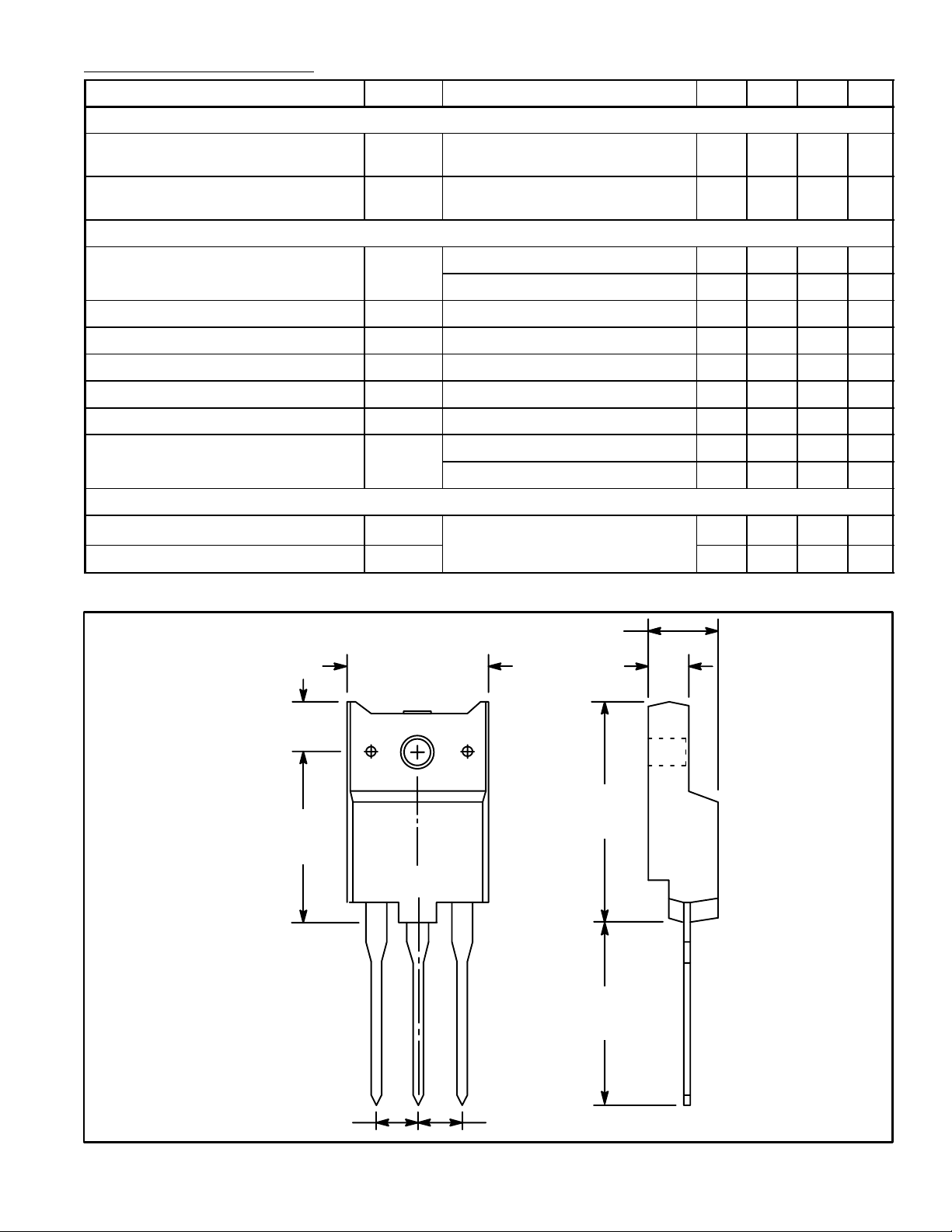
.228 (5.8) Max
.177
(4.5)
.885
(22.5)
Max
.630 (16.0) Max
Isol
E
C
B
.118 (3.0)
1.063
(27.0)
Max
.712
(18.1)
Min
.215 (5.45)
.215 (5.45)
 Loading...