

NTE NTE2638 Datasheet

NTE2638
Silicon NPN Transistor
Darlington
Features:
D High Voltage, High Forward and Clamped Reverse Energy
D 10A Peak Collector Current
D 80W at +25°C Case Temperature
D Collector–Emitter Sustaining Voltage: 400V Min at 7A
Absolute Maximum Ratings: (TC = +25°C unless otherwise specifieid)
Collector–Emitter Voltage (IB = 0), V
Collector–Base Voltage, V
Emitter–Base Voltage, V
Collector Current, I
C
CBO
EBO
Continuous 7A. . . . . . . . . . . . . . . . . . . . . . . . . . . . . . . . . . . . . . . . . . . . . . . . . . . . . . . . . . . . . . . . . . .
Peak (Note 1) 10A. . . . . . . . . . . . . . . . . . . . . . . . . . . . . . . . . . . . . . . . . . . . . . . . . . . . . . . . . . . . . . . .
Continuous Base Current, I
B
Continuous Device Dissipation (TC = +25°C), P
Derate Linearly to 150°C 0.64W/°C. . . . . . . . . . . . . . . . . . . . . . . . . . . . . . . . . . . . . . . . . . . . . . . . .
Continuous Device Dissipation (TA = +25°C), P
Derate Linearly to 150°C 16mW/°C. . . . . . . . . . . . . . . . . . . . . . . . . . . . . . . . . . . . . . . . . . . . . . . . .
Operating Junction Temperature Range, T
Storage Temperature Range, T
Thermal Resistance, Junction–to–Case, R
Thermal Resistance, Junction–to–Ambient, R
Typical Thermal Resistance, Case–to–Heat Sink (Note 2), R
Lead Temperature (During Soldering, 1/8” from case, 10sec), T
CEO
D
D
J
stg
thJC
thJA
thCHS
L
400V. . . . . . . . . . . . . . . . . . . . . . . . . . . . . . . . . . . . . . . . . . . . . .
400V. . . . . . . . . . . . . . . . . . . . . . . . . . . . . . . . . . . . . . . . . . . . . . . . . . . . . .
8V. . . . . . . . . . . . . . . . . . . . . . . . . . . . . . . . . . . . . . . . . . . . . . . . . . . . . . . . . .
1.5A. . . . . . . . . . . . . . . . . . . . . . . . . . . . . . . . . . . . . . . . . . . . . . . . . . . . . . . .
80W. . . . . . . . . . . . . . . . . . . . . . . . . . . . . . . . . . . . . .
2W. . . . . . . . . . . . . . . . . . . . . . . . . . . . . . . . . . . . . . .
–65° to +150°C. . . . . . . . . . . . . . . . . . . . . . . . . . . . . . . . . .
–65° to +150°C. . . . . . . . . . . . . . . . . . . . . . . . . . . . . . . . . . . . . . . . . .
1.56°C/W. . . . . . . . . . . . . . . . . . . . . . . . . . . . . . . . . . . .
62.5°C/W. . . . . . . . . . . . . . . . . . . . . . . . . . . . . . . . . .
0.7°C/W. . . . . . . . . . . . . . . . . . . .
+260°C. . . . . . . . . . . . . . . . . . . . . .
Note 1. This value applies for tw ≤ 5ms, duty cycle ≤ 10%.
Note 2. This parameter is measured using 0.003” (0.08mm) mica insulator with Dow–Corning 11
compound on both sides of the insulator, a 0.138–32 (formally 6–32) mounting screw with
bushing, and a mounting torque of 8 in•lb (0.9 n•m).
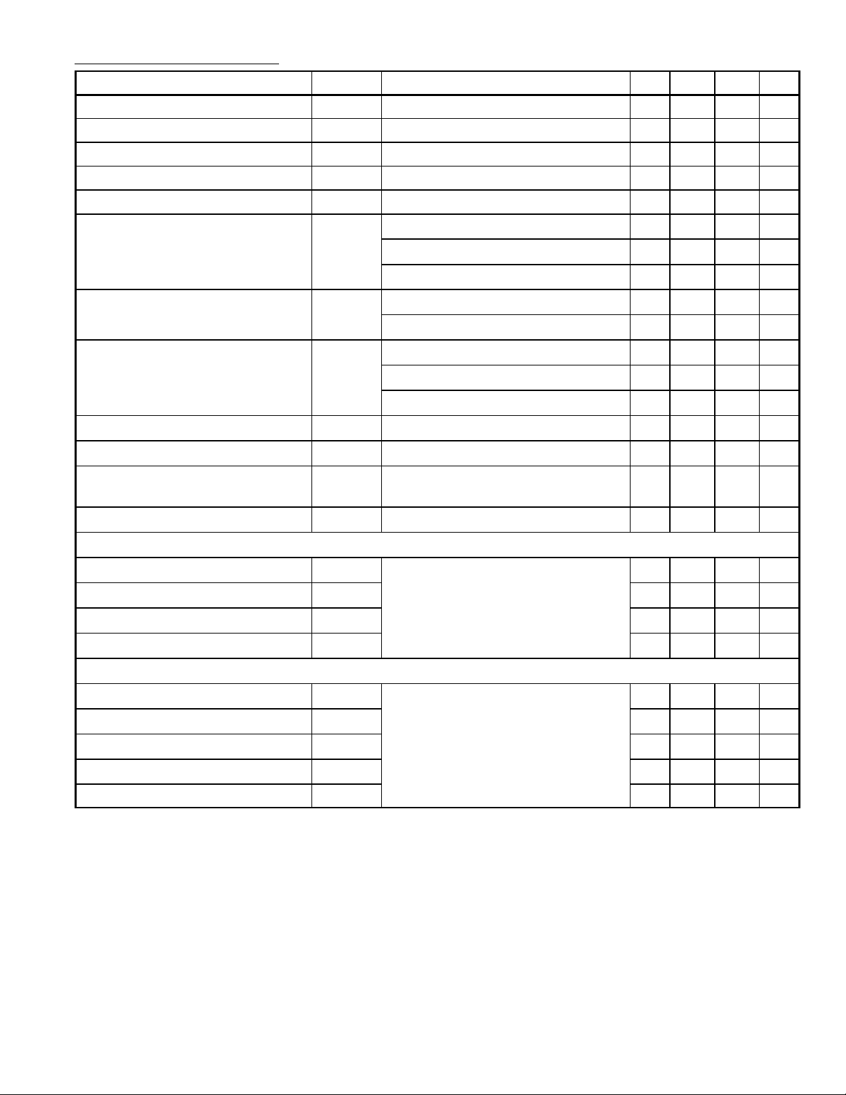
Electrical Characteristics: (TC = +25°C unless otherwise specified)
Parameter Symbol Test Conditions Min Typ Max Unit
Collector–Base Breakdown Voltage V
Collector–Emitter Breakdown Voltage V
Collector–Emitter Sustaining Voltage V
Collector Cutoff Current I
Emitter Cutoff Current I
(BR)CBOIC
(BR)CEOIC
CEX(sus)IC
CEO
EBO
DC Current Gain h
Base–Emitter Voltage V
Collector–Emitter Saturation
V
CE(sat)IB
Voltage
Diode Forward Voltage V
Small–Signal Current Gain h
Small–Signal Forward Current
|hfe| VCE = 5V, IC = 500mA, f = 1kHz 10 – –
Transfer Ratio
FE
BE
fe
= 1mA, IE = 0, Note 3 400 – – V
= 10mA, IB = 0, Note 3 400 – – V
= 7A 400 – – V
VCE = 400V, IB = 0 – – 250 µA
VEB = 8V, IC = 0 – – 15 mA
IC = 2.5A, VCE = 5V, Note 3, Note 4 150 – –
IC = 5A, VCE = 5V, Note 3, Note 4 50 – –
IC = 7A, VCE = 5V, Note 3, Note 4 15 – –
IB = 100mA, IC = 2A, Not e 3, Not e 4
– – 2.2 V
IB = 250mA, IC = 5A, Not e 3, Not e 4 – – 2.3 V
= 10mA, IC = 1A, Not e 3, Not e 4 – – 1.5 V
IB = 100mA, IC = 2A, Not e 3, Not e 4 – – 1.5 V
IB = 250mA, IC = 5A, Not e 3, Not e 4 – – 2.0 V
IF = 7A, Note 3, Note 4 – – 3.5 V
F
VCE = 5V, IC = 500mA, f = 1kHz 200 – –
Collector Capacitance C
obo
IE = 0, VCB = 10V, f = 1MHz – – 100 pF
Resistive–Load Switching Characteristics (TC = +25°C unless otherwise specified)
Turn–Off Storage Time t
Turn–Off Fall Time t
Turn–Off Rise Time t
Turn–On Delay Time t
IC = 5A, IB1 = 250mA,
s
IB2 = –250mA, V
f
RL = 50Ω, Note 5
R = 50Ω, Note 5
r
d
BE(off)
= –7.3V,
– 3400 – ns
– 1520 – ns
– 160 – ns
– 20 – ns
Inductive–Load Switching Characteristics (TC = +25°C unless otherwise specified)
Voltage Storage Time t
Current Storage Time t
Voltage Rise Time t
Storage Rise Time t
Turn–Off Crossover Time t
sv
rv
xo
V
(clamp)
= Min V
CEX(sus)
, ICM = 5A,
IB1 = 250mA, IB2 = –250mA,
si
Note 5
Note 5
ri
– 3900 – ns
– 4700 – ns
– 1200 – ns
– 1200 – ns
– 2000 – ns
Note 3. These parameters must be measured using pulse techniques, tw = 300µs, duty cycle ≤ 2%.
Note 4. These parameters are measured with voltage–sensing contacts separate from the current–
carrying contacts located within 1/8” (3.2mm) from the device body.
Note 5. Voltage and current values shown are nominal; exact values vary slightly with transistor pa-
rameters.
 Loading...