

NTE NTE2635 Datasheet
NTE2635
Silicon NPN Transistor
w
Horizontal Deflection
Description:
The NTE2635 is an enhanced performance, new generation, high–voltage, high–speed switching
NPN transistor with an integrated damper diode in a full–pack envelope intended for use in horizontal
deflection circuits in color TV receivers. This device features exceptional tolerance to base drive and
collector current load variations resulting in a very low worst case dissipation.
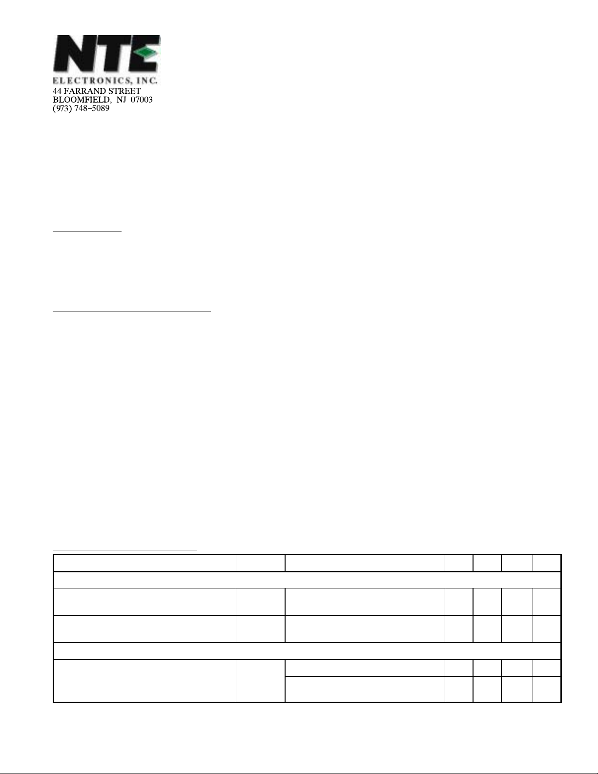
Absolute Maximum Ratings:
Collector–Emitter Voltage (VBE = 0V), V
Collector–Emitter Voltage, V
Collector Current, I
C
CEO
Continuous 8A. . . . . . . . . . . . . . . . . . . . . . . . . . . . . . . . . . . . . . . . . . . . . . . . . . . . . . . . . . . . . . . . . . .
Peak 15A. . . . . . . . . . . . . . . . . . . . . . . . . . . . . . . . . . . . . . . . . . . . . . . . . . . . . . . . . . . . . . . . . . . . . . .
Base Current, I
B
Continuous 4A. . . . . . . . . . . . . . . . . . . . . . . . . . . . . . . . . . . . . . . . . . . . . . . . . . . . . . . . . . . . . . . . . . .
Peak 6A. . . . . . . . . . . . . . . . . . . . . . . . . . . . . . . . . . . . . . . . . . . . . . . . . . . . . . . . . . . . . . . . . . . . . . . .
Reverse Base Current, –I
B
Continuous (Average over any 20ms period) 100mA. . . . . . . . . . . . . . . . . . . . . . . . . . . . . . . . . .
Peak (Turn–Off Current) 5A. . . . . . . . . . . . . . . . . . . . . . . . . . . . . . . . . . . . . . . . . . . . . . . . . . . . . . . .
Total Power Dissipation (T
= +25°C), P
C
Operating Junction Temperature, T
Storage Temperature Range, T
stg
Thermal Resistance, Junction–to–Case (With Heat Sink Compound), R
Typical Thermal Resistance, Junction–to–Ambient, R
CESM
tot
J
/Internal Damper Diode
thJC
thJA
1500V. . . . . . . . . . . . . . . . . . . . . . . . . . . . . . . . . . . . . . . .
700V. . . . . . . . . . . . . . . . . . . . . . . . . . . . . . . . . . . . . . . . . . . . . . . . . . . . .
35W. . . . . . . . . . . . . . . . . . . . . . . . . . . . . . . . . . . . . . . . . . . .
+150°C. . . . . . . . . . . . . . . . . . . . . . . . . . . . . . . . . . . . . . . . . . . . . . .
–65° to +150°C. . . . . . . . . . . . . . . . . . . . . . . . . . . . . . . . . . . . . . . . . .
3.6K/W. . . . . . . . . . . . .
55K/W. . . . . . . . . . . . . . . . . . . . . . . . . . . . .
Electrical Characteristics:
Parameter Symbol Test Conditions Min Typ Max Unit
Isolation Limiting Value
RMS Isolation Voltage from all
Three Terminals to Case
Capacitance from T2 to External
Heat Sink
Static Characteristics
Collector Cutoff Current I
(TC = +25°C unless otherwise specified)
V
C
ISOL
ISOL
CES
f = 50–60hz, Sinusoidal Waveform,
R.H. ≤ 65%, Clean and Dustfree
f = 1MHz – 10 – pF
VCE = 1500V, VBE = 0, Note 1 – – 1.0 mA
VCE = 1500V, VBE = 0, TJ = +125°C,
Note 1
Note 1. Measured with half sine–wave voltage (curve tracer).
– – 2500 V
– – 2.0 mA
Electrical Characteristics: (TC = +25°C unless otherwise specified)
Parameter Symbol Test Conditions Min Typ Max Unit
Static Characteristics (Cont’d)
Emitter Cutoff Current I
Emitter–Base Breakdown Voltage V
EBO
(BR)EBOIB
Base–Emitter Resistance R
Collector–Emitter Sustaining Voltage V
Collector–Emitter Saturation Voltage V
Base–Emitter Saturation Voltage V
CEO(sus)IB
CE(sat)IC
BE(sat)IC
DC Current Gain h
Diode Forward Voltage V
Dymanic Characteristics
Collector Capacitance C
Turn–Off Storage Time t
Turn–Off Fall Time t
Max
.114 (2.9)
be
FE
s
VEB = 7.5V, IC = 0 140 – 390 mA
= 600mA 7.5 13.5 – V
VEB = 7.5V – 33 – Ω
= 0, IC = 100mA, L = 25mH 700 – – V
= 4.5A, IB = 1.1A – – 5.0 V
IC = 4.5A, IB = 1.29A – – 1.0 V
= 4.5A, IB = 1.7A – – 1.3 V
IC = 1A, VCE = 5V 7 13 23
IC = 4.5A, VCE = 1V 4.0 5.5 7.5
IF = 4.5A – 1.6 2.0 V
F
IE = 0, VCB = 10V, f = 1MHz – 80 – pF
c
IC = 4.5A Peak, I
B(end)
= 1.1A,
– 5.0 6.0 µs
LB = 6µH, –VBB = 4V,
f
.126 (3.2) Dia Max.181 (4.6)
(–dI
/dt = 0.6A/µs)
B
.405 (10.3)
Max
– 0.4 0.6 µs
.252
(6.4)
.531
(13.5)
Min
.622
(15.0)
Max
.118
(3.0)
Max
Isol
COLLECTOR
BASE
BC E
EMITTER
.100 (2.54).098 (2.5)
 Loading...