

NTE NTE2634, NTE2633 Datasheet
NTE2633 (NPN) & NTE2634 (PNP)
Silicon Complementary Transistors
High Frequency Video Driver
Description:
The NTE2633 (NPN) and NTE2634 (PNP) are silicon complementary epitaxial transistor in a TO126
type package designed for use in the buffer stage of the driver for high–resolution color graphics monitors.
Features:
D High Breakdown Voltage
D Low Output Capacitance
Absolute Maximum Ratings:
Collector–Base Voltage, V
Collector–Emitter Voltage, V
Collector–Emitter Voltage (R
Emitter–Base Voltage, V
DC Collector Current, I
Total Power Dissipation (T
Operating Junction Temperature, T
Storage Temperature Range, T
CBO
CEO
= 100Ω), V
BE
EBO
C
≤ +115°C, Note 1), P
S
J
stg
CER
tot
Thermal Resistance, Junction–to–Soldering Point (T
≤ +115°C, Note 1), R
S
–65° to +175°C. . . . . . . . . . . . . . . . . . . . . . . . . . . . . . . . . . . . . . . . . .
thJS
115V. . . . . . . . . . . . . . . . . . . . . . . . . . . . . . . . . . . . . . . . . . . . . . . . . . . . . .
95V. . . . . . . . . . . . . . . . . . . . . . . . . . . . . . . . . . . . . . . . . . . . . . . . . . . . . .
110V. . . . . . . . . . . . . . . . . . . . . . . . . . . . . . . . . . . . . . . .
3V. . . . . . . . . . . . . . . . . . . . . . . . . . . . . . . . . . . . . . . . . . . . . . . . . . . . . . . . . .
300mA. . . . . . . . . . . . . . . . . . . . . . . . . . . . . . . . . . . . . . . . . . . . . . . . . . . . . . . . . .
3W. . . . . . . . . . . . . . . . . . . . . . . . . . . . . . . . . . . . .
+175°C. . . . . . . . . . . . . . . . . . . . . . . . . . . . . . . . . . . . . . . . . . . . . . .
20K/W. . . . . . . . .
Note 1. T
Electrical Characteristics:
Collector–Base Breakdown Voltage V
Collector–Emitter Breakdown Voltage V
Emitter–Base Breakdown Voltage V
Collector Cutoff Current I
DC Current Gain h
Transition Frequency f
Collector–Base Capacitance C
is the temperature at the soldering point of the collector lead.
S
(TJ = +25°C unless otherwise specified)
Parameter Symbol Test Conditions Min Typ Max Unit
V
(BR)CBOIC
(BR)CEOIC
(BR)CERIC
(BR)EBOIE
CES
I
CBO
FE
T
cb
IB = 0, VCE = 50V – – 100 µA
IE = 0, VCB = 50V – – 20 µA
IC = 50mA, VCE = 10V, TA = +25°C 20 35 –
IC = 50mA, VCE = 10V, f = 100MHz,
T
IC = 0, VCB = 10V, f = 1MHz, TA = +25°C – 2.0 – pF
= 0.1mA 115 – – V
= 10mA 95 – – V
= 10mA, RBE = 100Ω 110 – – V
= 0.1mA 3 – – V
0.8 1.2 – GHz
= +25°C
A
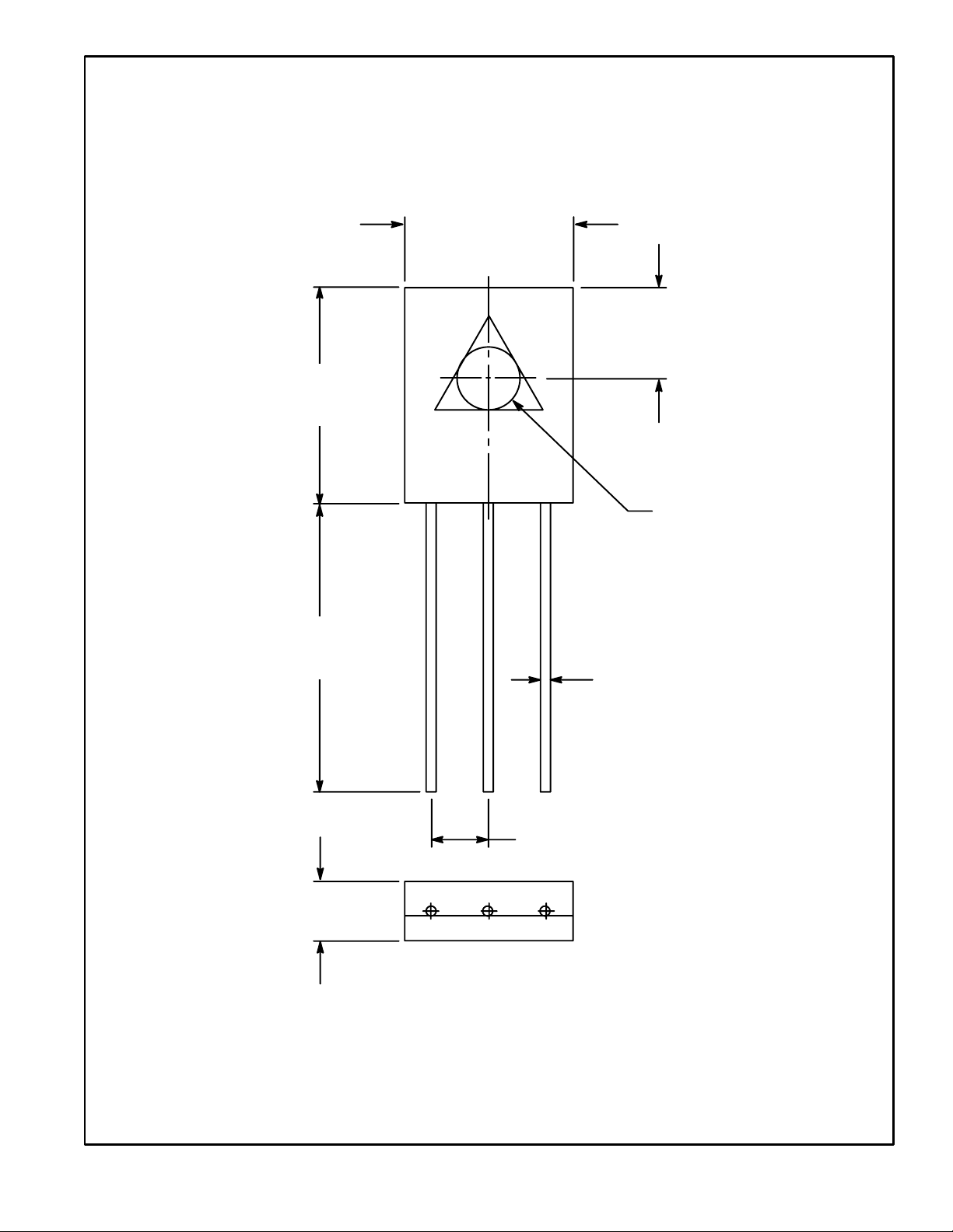
.450
(11.4)
Max
.655
(16.6)
Max
.330 (8.38) Max
.175
(4.45)
Max
.118
(3.0)
Dia
.030 (.762) Dia
.130 (3.3)
Max
ECB
.090 (2.28)
 Loading...