

NTE NTE2631 Datasheet

NTE2631
Integrated Circuit
Quad Differential Line Driver
Functional Description:
The NTE2631 is a quad differential line driver constructed using Advanced Low–Power Schottky
processing in a 16–Lead DIP type package designed for digital data transmission over balanced lines.
This device meets all the requirements of EIA standard RS–422 and federal standard 1020 and is
designed to provide unipolar differential drive to twisted–pair or parallel–wire transmission lines.
The NTE2631 provides an enable and disable function common to all four drivers and features
3–state outputs and logical OR–ed complemtary enable inputs. The inputs are all LS cxompatible
and are all one unit load.
Features:
D 2.0ns Output Skew Typical
D Operation from Single +5V Supply
D Output won’t Load Line when V
D Four Line Drivers in One Package for Maximum Package Density
D Output Short–Circuit Protection
D Complementary Outputs
D Meets the Requirements of EIA Standard RS–422
D High Output Drive Capability for 100Ω Terminated Transmission Lines
D Advanced Low–Power Schottky Processing
CC
= 0
Absolute Maximum Ratings
Supply Voltage 7.0V. . . . . . . . . . . . . . . . . . . . . . . . . . . . . . . . . . . . . . . . . . . . . . . . . . . . . . . . . . . . . . . . . . . .
Input Voltage 7.0V. . . . . . . . . . . . . . . . . . . . . . . . . . . . . . . . . . . . . . . . . . . . . . . . . . . . . . . . . . . . . . . . . . . . .
Output Voltage 5.5V. . . . . . . . . . . . . . . . . . . . . . . . . . . . . . . . . . . . . . . . . . . . . . . . . . . . . . . . . . . . . . . . . . . .
Storage Temperature Range –65°C to +165°C. . . . . . . . . . . . . . . . . . . . . . . . . . . . . . . . . . . . . . . . . . . .
: (above which the useful life may be impaired)
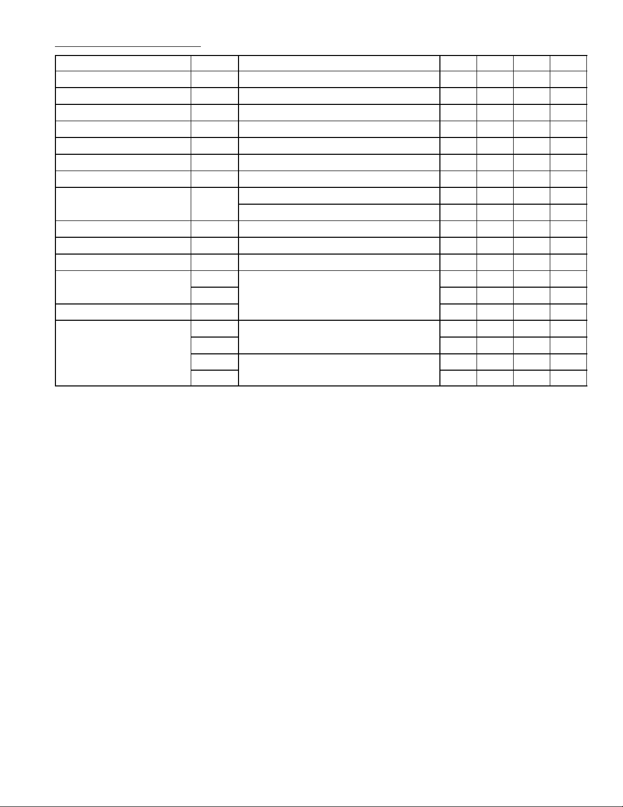
Electrical Characteristics: (VCC = 5V ±5%, TA = 0° to +70°C, Note 1 unless otherwise specified)
Parameter Symbol Test Conditions Min Typ Max Unit
Output HIGH Voltage V
OH
Output LOW Voltage V
Input HIGH Voltage V
Input LOW Voltage V
Input LOW Current I
Input HIGH Current I
IH
Input Reverse Current I
Off–State (High Impedance) I
Output Current
Input Clamp Voltage V
Output Short Circuit Current I
Power Supply Current I
Input to Output t
CC
PLH
t
PHL
SC
Output to Output SKEW – 2.0 6.0 ns
Enable to Output t
t
t
t
LZ
HZ
ZL
ZH
VCC = Min, IOH = –20mA 2.5 3.2 – V
VCC = Min, IOL = 20mA – 0.32 0.5 V
OL
VCC = Min 2.0 – – V
IH
VCC = Max – – 0.8 V
IL
VCC = Max, VIN = 0.4V – –0.20 –0.36 mA
IL
V
= Max, VIN = 2.7V – 0.5 20 µA
CC
VCC = Max, VIN = 7.0V – 0.001 0.1 mA
I
VCC = Max, VO = 5.5V – 0.5 20 µA
O
V
= Max, VO = 0.5V – 0.5 –20 µA
CC
VCC = Min, IIN = 18mA – –0.8 –1.5 V
I
VCC = Max –30 –60 –150 mA
VCC = Max, all outputs disabled – 60 80 mA
VCC = 5V, TA = +25°C, Load = Note 2 – 12 20 ns
– 12 20 ns
VCC = 5V, TA = +25°C, CL = 10pF – 23 35 ns
– 17 30 ns
VCC = 5V, TA = +25°C, Load = Note 2 – 35 45 ns
– 30 40 ns
Note 1. All typical values are VCC = 5V, TA = +25°C.
Note 2. C
= 30pF, VIN = 1.3V to V
L
= 1.3V, V
OUT
PULSE
= 0V to +3.0V.
 Loading...