

NTE NTE2597 Datasheet
Silicon NPN Transistor
High Voltage, High Speed Switch
Features:
D High Breakdown Voltage and Reliability
D Fast Switching Speed
D Wide ASO
NTE2597
Absolute Maximum Ratings:
Collector–Base Voltage, V
Collector–Emitter Voltage, V
Emitter–Base Voltage, V
Collector Current, I
EBO
C
(TA = +25°C unless otherwise specified)
CBO
CEO
Continuous 12A. . . . . . . . . . . . . . . . . . . . . . . . . . . . . . . . . . . . . . . . . . . . . . . . . . . . . . . . . . . . . . . . . .
Peak (Note 1) 30A. . . . . . . . . . . . . . . . . . . . . . . . . . . . . . . . . . . . . . . . . . . . . . . . . . . . . . . . . . . . . . . .
Base Current, I
Collector Dissipation, P
B
D
TA = +25°C 3W. . . . . . . . . . . . . . . . . . . . . . . . . . . . . . . . . . . . . . . . . . . . . . . . . . . . . . . . . . . . . . . . . .
TC = +25°C 65W. . . . . . . . . . . . . . . . . . . . . . . . . . . . . . . . . . . . . . . . . . . . . . . . . . . . . . . . . . . . . . . . .
Operating Junction Temperature, T
Storage Temperature Range, T
J
stg
Note 1. Pulse Test: Pulse Width ≤ 300µs, Duty Cycle ≤ 10%.
Electrical Characteristics:
Parameter Symbol Test Conditions Min Typ Max Unit
Collector Cutoff Current I
Emitter Cutoff Current I
DC Current Gain h
(TA = +25°C unless otherwise specified)
CBO
EBO
FE
VCB = 800V, IE = 0 – – 10 µA
VEB = 5V, IC = 0 – – 10 µA
VCE = 5V, IC = 0.8A 10 – 40
VCE = 5V, IC = 4A 8 – –
1100V. . . . . . . . . . . . . . . . . . . . . . . . . . . . . . . . . . . . . . . . . . . . . . . . . . . . .
800V. . . . . . . . . . . . . . . . . . . . . . . . . . . . . . . . . . . . . . . . . . . . . . . . . . . . .
7V. . . . . . . . . . . . . . . . . . . . . . . . . . . . . . . . . . . . . . . . . . . . . . . . . . . . . . . . . .
6A. . . . . . . . . . . . . . . . . . . . . . . . . . . . . . . . . . . . . . . . . . . . . . . . . . . . . . . . . . . . . . . . . . . .
+150°C. . . . . . . . . . . . . . . . . . . . . . . . . . . . . . . . . . . . . . . . . . . . . . .
–55° to +150°C. . . . . . . . . . . . . . . . . . . . . . . . . . . . . . . . . . . . . . . . . .
Collector–Emitter Saturation Voltage V
Base–Emitter Saturation Voltage V
CE(sat)IC
BE(sat)IC
= 6A, IB = 1.2A – – 2.0 V
= 6A, IB = 1.2A – – 1.5 V
Electrical Characteristics (Cont’d): (TA = +25°C unless otherwise specified)
Parameter Symbol Test Conditions Min Typ Max Unit
Gain–Bandwidth Product f
Output Capacitance C
Collector–Base Breakdown Voltage V
Collector–Emitter Breakdown Voltage V
Emitter–Base Breakdown Voltage V
Collector–Emitter Sustaining Voltage V
(BR)CBOIC
(BR)CEOIC
(BR)EBOIE
CEX(sus)IC
Turn–On Time t
Storage Time t
Fall Time t
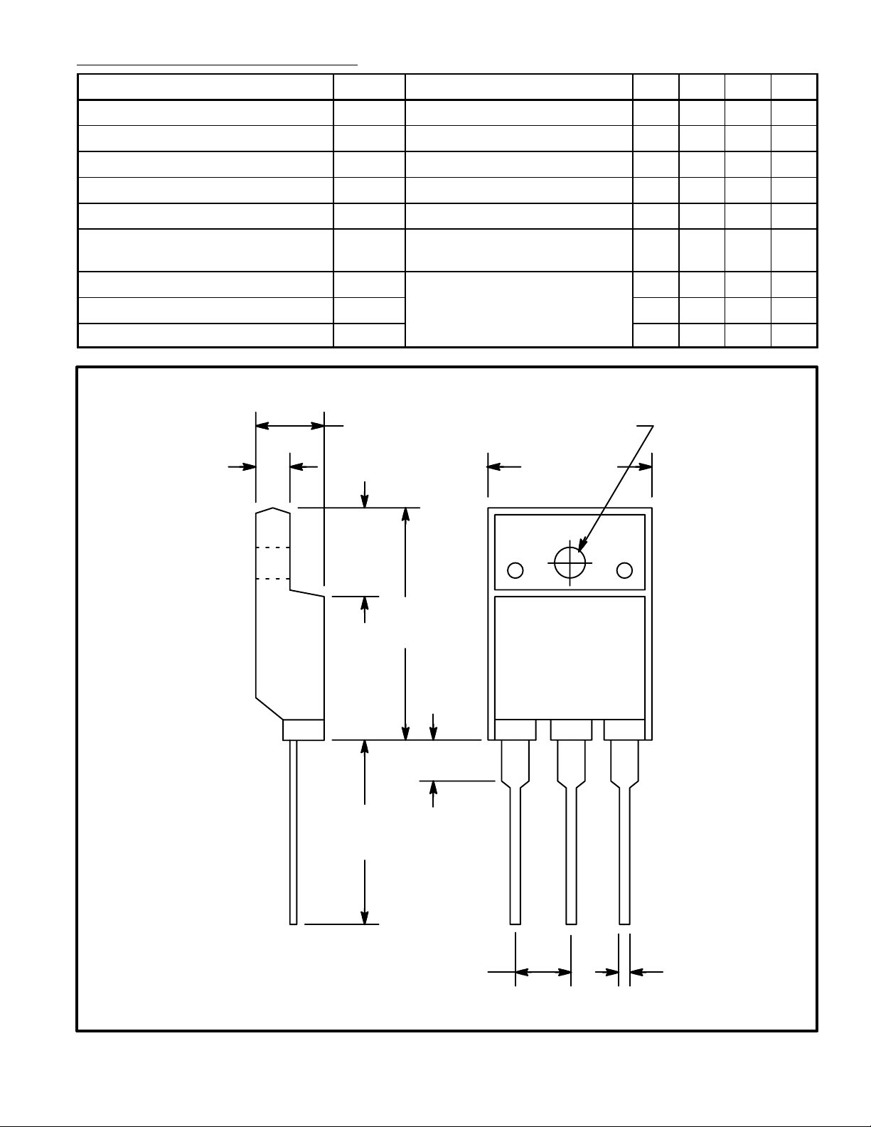
.221 (5.6)
.123 (3.1)
on
stg
T
ob
VCE = 10V, IC = 0.8A – 15 – MHz
VCB = 10V, f = 1MHz – 215 – pF
= 1mA, IE = 0 1100 – – V
= 10mA, RBE = ∞ 800 – – V
= 1mA, IC = 0 7 – – V
= 6A, IB1 = 1.2A, IB2 = –1.2A,
800 – – V
L = 500µH Clamped
IC = 8A, IB1 = 1.6A,
IB2 = –3.2A, RL = 50Ω,
V = 400V
VCC = 400V
f
– – 0.5 µs
– – 3.0 µs
– – 0.3 µs
.134 (3.4) Dia
.630 (16.0)
.315
(8.0)
.804
(20.4)
.866
(22.0)
BCE
.158 (4.0)
.215 (5.45) .040 (1.0)
 Loading...