

NTE NTE2540 Datasheet
NTE2540
Silicon NPN Transistor
Darlington, High Voltage Switch
Features:
D High DC Current Gain: hFE = 600 Min (VCE = 2V, IC = 2A)
D Monolithic Construction
w
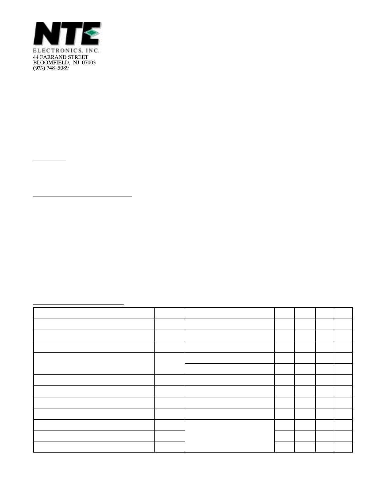
/Built–In Base–Emitter Shunt Resistor
Absolute Maximum Ratings:
Collector Base Voltage, V
Collector Emitter Voltage, V
Emitter Base Voltage, V
Collector Current, I
Base Current. I
B
EBO
C
Collector Power Dissipation, P
(TA = +25°C unless otherwise specified)
CBO
CEO
C
TA = +25°C 2W. . . . . . . . . . . . . . . . . . . . . . . . . . . . . . . . . . . . . . . . . . . . . . . . . . . . . . . . . . . . . . . . . .
TC = +25°C 25W. . . . . . . . . . . . . . . . . . . . . . . . . . . . . . . . . . . . . . . . . . . . . . . . . . . . . . . . . . . . . . . . .
Operating Junction Temperature, T
Storage Temperature Range, T
Electrical Characteristics:
Parameter Symbol Test Conditions Min Typ Max Unit
Collector Cutoff Current I
Emitter Cutoff Current I
Collector–Emitter Breakdown Voltage V
DC Current Gain h
(TA = +25°C unless otherwise specified)
J
stg
CBO
EBO
(BR)CEOIC
FE
VCB = 600V, IE = 0 – – 0.5 mA
VEB = 5V, IC = 0 – – 3 mA
VCE = 2V, IC = 2A 600 – –
VCE = 2V, IC = 4A 100 – –
600V. . . . . . . . . . . . . . . . . . . . . . . . . . . . . . . . . . . . . . . . . . . . . . . . . . . . . . .
400V. . . . . . . . . . . . . . . . . . . . . . . . . . . . . . . . . . . . . . . . . . . . . . . . . . . . .
5V. . . . . . . . . . . . . . . . . . . . . . . . . . . . . . . . . . . . . . . . . . . . . . . . . . . . . . . . . . .
6A. . . . . . . . . . . . . . . . . . . . . . . . . . . . . . . . . . . . . . . . . . . . . . . . . . . . . . . . . . . . . . . . .
1A. . . . . . . . . . . . . . . . . . . . . . . . . . . . . . . . . . . . . . . . . . . . . . . . . . . . . . . . . . . . . . . . . . . .
+150°C. . . . . . . . . . . . . . . . . . . . . . . . . . . . . . . . . . . . . . . . . . . . . . .
–55° to +150°C. . . . . . . . . . . . . . . . . . . . . . . . . . . . . . . . . . . . . . . . . .
= 10mA, IB = 0 400 – – V
Collector–Emitter Saturation Voltage V
Base–Emitter Saturation Voltage V
Emitter–Collector Forward Voltage V
Collector Output Capacitance C
Turn–On Time t
Storage Time t
Fall Time t
CE(sat)IC
BE(sat)IC
ECF
ob
on
stg
f
= 4A, IB = 40mA – – 2.0 V
= 4A, IB = 40mA – – 2.5 V
IE = 4A, IB = 0 – – 3.0 V
VCB = 50V, IE = 0, f = 1MHz – 35 – pF
VCC = 100V,
IB1 = –IB2 = 40mA,
Duty Cycle ≤ 1%
Duty Cycle ≤ 1%
– 1 – µs
– 8 – µs
– 5 – µs
Darlington Internal Schematic
B
C
E
.402 (10.2) Max
.224 (5.7) Max
.669
(17.0)
Max
.531
(13.5)
Min
.295
(7.5)
BCE
.122 (3.1)
Dia
.165
(4.2)
.173 (4.4)
Max
.114 (2.9)
Max
.100 (2.54) .059 (1.5) Max
 Loading...