

NTE NTE2503 Datasheet
NTE2503
Silicon NPN Transistor
High Gain Switch
Features:
D High DC Current Gain
D High Current Capacity
D Low Collector–Emitter Saturation Voltage
D High Emitter–Base Voltage
Applications:
D AF Amplifier
D Various Driver
Absolute Maximum Ratings:
Collector–Emitter Voltage, V
Collector–Base Voltage, V
Emitter–Base Voltage, V
Collector Current, I
EBO
C
(TA = +25°C unless otherwise specified)
CEO
CBO
Continuous 700mA. . . . . . . . . . . . . . . . . . . . . . . . . . . . . . . . . . . . . . . . . . . . . . . . . . . . . . . . . . . . . . .
Pulse 1.5A. . . . . . . . . . . . . . . . . . . . . . . . . . . . . . . . . . . . . . . . . . . . . . . . . . . . . . . . . . . . . . . . . . . . . .
Collector Dissipation, P
Operating Junction Temperature, T
Storage Temperature Range, T
Electrical Characteristics:
Parameter Symbol Test Conditions Min Typ Max Unit
Collector Cutoff Current I
Emitter Cutoff Current I
DC Current Gain h
Current Gain–Bandwidth Product f
Output Capacitance C
C
J
stg
(TA = +25°C unless otherwise specified)
CBO
EBO
FE
T
ob
25V. . . . . . . . . . . . . . . . . . . . . . . . . . . . . . . . . . . . . . . . . . . . . . . . . . . . . .
30V. . . . . . . . . . . . . . . . . . . . . . . . . . . . . . . . . . . . . . . . . . . . . . . . . . . . . . .
15V. . . . . . . . . . . . . . . . . . . . . . . . . . . . . . . . . . . . . . . . . . . . . . . . . . . . . . . . .
600mW. . . . . . . . . . . . . . . . . . . . . . . . . . . . . . . . . . . . . . . . . . . . . . . . . . . . . . . .
+150°C. . . . . . . . . . . . . . . . . . . . . . . . . . . . . . . . . . . . . . . . . . . . . . .
–55° to +150°C. . . . . . . . . . . . . . . . . . . . . . . . . . . . . . . . . . . . . . . . . .
VCB = 20V, IE = 0 – – 0.1 µA
VEB = 10V, IC = 0 – – 0.1 µA
IC = 50mA, VCE = 5V 800 1500 3200
IC = 500mA, VCE = 5V 600 – –
IC = 50mA, VCE = 10V – 270 – MHz
VCB = 10V, f = 1MHz – 9 – pF
Electrical Characteristics (Cont’d): (TA = +25°C unless otherwise specified)
µ
Parameter Symbol Test Conditions Min Typ Max Unit
Collector Saturation Voltage V
Base Saturation Voltage V
Collector–Base Breakdown Voltage V
Collector–Emitter Breakdown Voltage V
Emitter–Base Breakdown Voltage V
Turn–On Time t
Storage Time t
Fall Time t
CE(sat)IC
BE(sat)IC
(BR)CBOIC
(BR)CEOIC
(BR)EBOIE
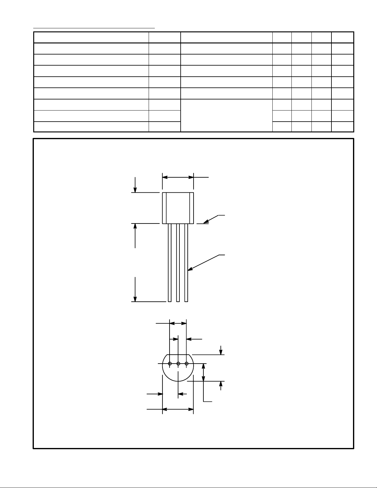
.210
(5.33)
Max
on
stg
= 500mA, IB = 10mA – 0.15 0.50 V
= 500mA, IB = 10mA – 0.9 1.2 V
= 10µA, IE = 0 30 – – V
= 1mA, RBE = ∞ 25 – – V
= 10µA, IC = 0 15 – – V
IB1 = 100mA,
IB2 = IC = 300mA,
Pulse Width = 20
Pulse Width = 20µs,
Duty Cycle ≤ 1%
f
s,
.135 (3.45) Min
Seating Plane
– 0.1 – µs
– 0.6 – µs
– 0.06 – µs
.500
(12.7)
Min
.100 (2.54)
.105 (2.67) Max
.205 (5.2) Max
.021 (.445) Dia Max
E C B
.050 (1.27)
.165
(4.2)
Max
.105 (2.67) Max
 Loading...