

NTE NTE2402, NTE2403 Datasheet
NTE2402 (NPN) & NTE2403 (PNP)
Silicon Complementary Transistors
Low Noise, UHF/VHF Amplifier
Description:
The NTE2402 (NPN) and NTE2403 (PNP) are silicon complementary transistors in an SOT–23 type
surface mount package designed for use in UHF and microwave amplifiers in thick and thin–film circuits, such as in aerial amplifiers, radar systems, oscilloscopes, spectrum analysers, etc. These transistors feature low intermodulation distortion and high power gain. Due to very high transition frequency, these devices also have excellent wideband properties and low noise up to high frequencies.
Absolute Maximum Ratings:
Collector–Base Voltage, V
Collector–Emitter Voltage, V
Emitter–Base Voltage, V
DC Collector Current, I
Total Power Dissipation (T
Operating Junction Temperature, T
Storage Temperature Range, T
CBO
CEO
EBO
C
≤ +60°C, Note 1), P
A
J
stg
tot
Thermal Resistance, Junction–to–Ambient (Note 1), R
–65° to +150°C. . . . . . . . . . . . . . . . . . . . . . . . . . . . . . . . . . . . . . . . . .
thJA
20V. . . . . . . . . . . . . . . . . . . . . . . . . . . . . . . . . . . . . . . . . . . . . . . . . . . . . . .
15V. . . . . . . . . . . . . . . . . . . . . . . . . . . . . . . . . . . . . . . . . . . . . . . . . . . . . .
2V. . . . . . . . . . . . . . . . . . . . . . . . . . . . . . . . . . . . . . . . . . . . . . . . . . . . . . . . . .
25mA. . . . . . . . . . . . . . . . . . . . . . . . . . . . . . . . . . . . . . . . . . . . . . . . . . . . . . . . . . .
200mW. . . . . . . . . . . . . . . . . . . . . . . . . . . . . . . . . .
+150°C. . . . . . . . . . . . . . . . . . . . . . . . . . . . . . . . . . . . . . . . . . . . . . .
430K/W. . . . . . . . . . . . . . . . . . . . . . . . . . .
Note 1. Mounted on a ceramic substrate of .314 (8mm) x .393 (10mm) x .027 (0.7mm).
Electrical Characteristics:
Parameter Symbol Test Conditions Min Typ Max Unit
Collector Cutoff Current I
DC Current Gain h
Transition Frequency f
Collector Capacitance C
Emitter Capacitance C
Feedback Capacitance C
(TJ = +25°C unless otherwise specified)
CBO
FE
VCB = 10V, IE = 0 – – 50 nA
VCE = 10V, IC = 14mA 25 50 –
VCE = 10V, IC = 14mA, f = 500MHz – 5 – GHz
T
VCB = 10V, IE = Ie = 0, f = 1MHz – 0.75 – pF
c
VEB = 0.5V, IC = Ic = 0, f = 1MHz – 0.8 – pF
e
VCE = 10V, IC = 2mA, f = 1MHz,
re
T
= +25°C
A
– 0.4 – pF
Electrical Characteristics (Cont’d): (TJ = +25°C unless otherwise specified)
Parameter Symbol Test Conditions Min Typ Max Unit
Noise Figure (At Optimum
Source Impedance)
Max. Unilateral Power Gain
(s
Assumed to be Zero)
re
Output Voltage
(At d
= –60dB)
im
F VCE = 10V, IC = 2mA, f = 500MHz,
T
= +25°C
A
G
UM
V
VCE = 10V, IC = 2mA, f = 500MHz,
T
= +25°C, Note 2
A
VCE = 10V, IC = 14mA, RL = 75Ω,
O
T
= +25°C, f
A
Note 2. GUM = 10 log |sfe|2 / [1 – |sie|2] [1 – |soe|2].
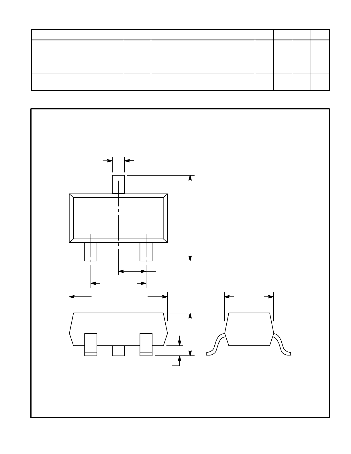
.016 (0.48)
C
B
E
(p+q–r)
.098
(2.5)
Max
– 2.4 – dB
– 18 – dB
– 150 – mV
= 493,25MHz
.074 (1.9)
.118 (3.0) Max
.037 (0.95)
.051
(1.3)
.043 (1.1)
.007 (0.2)
 Loading...