

NTE NTE2393 Datasheet

NTE2393
MOSFET
N–Channel Enhancement Mode,
High Speed Switch
Description:
The NTE2393 is an N–Channel Enhancement Mode Power MOS Field Effect Transistor. Easy drive
and very fast switching times make this device ideal for high speed switching applications. Typical
applications include switching mode power supplies, uninterruptible power supplies, and motor
speed control.
Features:
D High Voltage: 500V for Off–Line SMPS
D High Current: 9A for up to 350W SMPS
D Ultra Fast Switching for Operation at less than 100kHz
Industrial Applications:
D Switching Mode Power Supplies
D Motor Controls
Absolute Maximum Ratings:
Drain–Source Voltage (VGS = 0), V
Drain–Gate Voltage (R
Gate–Source Voltage, V
Continuous Drain Current, I
= 20kΩ), V
GS
GS
D
DS
DGR
TC = +25°C 9A. . . . . . . . . . . . . . . . . . . . . . . . . . . . . . . . . . . . . . . . . . . . . . . . . . . . . . . . . . . . . . . . . . .
T
= +100°C 5.6A. . . . . . . . . . . . . . . . . . . . . . . . . . . . . . . . . . . . . . . . . . . . . . . . . . . . . . . . . . . . . . . .
C
Pulsed Drain Current (Note 1), I
Clamped Drain Inductive Current (Note 1), I
Total Dissipation (T
= +25°C), P
C
DM
DLM
tot
Derate Above 25°C 1.2W/°C. . . . . . . . . . . . . . . . . . . . . . . . . . . . . . . . . . . . . . . . . . . . . . . . . . . . . . .
Maximum Operating Junction Temperature, T
Storage Temperature Range, T
stg
J
Maximum Thermal Resistance, Junction–to–Case, R
Maximum Lead Temperature (During Soldering), T
L
Note 1. Pulse width limited by safe operating area.
thJC
500V. . . . . . . . . . . . . . . . . . . . . . . . . . . . . . . . . . . . . . . . . . . . . . . .
500V. . . . . . . . . . . . . . . . . . . . . . . . . . . . . . . . . . . . . . . . . . . . .
±20V. . . . . . . . . . . . . . . . . . . . . . . . . . . . . . . . . . . . . . . . . . . . . . . . . . . . . . . . .
36A. . . . . . . . . . . . . . . . . . . . . . . . . . . . . . . . . . . . . . . . . . . . . . . . . . .
36A. . . . . . . . . . . . . . . . . . . . . . . . . . . . . . . . . . . . . . . .
150W. . . . . . . . . . . . . . . . . . . . . . . . . . . . . . . . . . . . . . . . . . . . . . . . .
+150°C. . . . . . . . . . . . . . . . . . . . . . . . . . . . . . . . . . . . . .
–65° to +150°C. . . . . . . . . . . . . . . . . . . . . . . . . . . . . . . . . . . . . . . . . .
0.83°C/W. . . . . . . . . . . . . . . . . . . . . . . . . . .
+275°C. . . . . . . . . . . . . . . . . . . . . . . . . . . . . . . . .
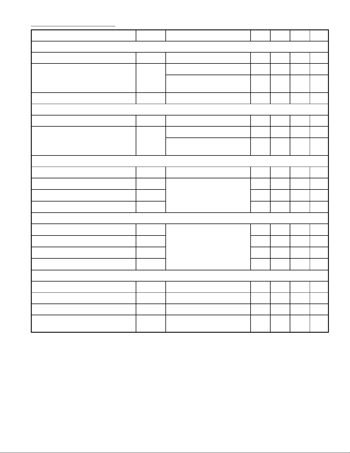
Electrical Characteristics: (TC = +25°C unless otherwise specified)
Parameter Symbol Test Conditions Min Typ Max Unit
OFF Characteristics
Drain–Source Breakdown Voltage V
(BR)DSSID
Zero–Gate Voltage Drain Current I
Gate–Body Leakage Current I
ON Characteristics (Note 2)
Gate Threshold Voltage V
Static Drain–Source On Resistance R
GS(th)
DS(on)VGS
Dynamic Characteristics
Forward Transconductance g
Input Capactiance C
Output Capacitance C
Reverse Transfer Capactiance C
Switching Characteristics
DSS
GSS
fs
iss
oss
rss
= 250µA, VGS = 0 500 – – V
VGS = 0, VDS = Max Rating – – 250 µA
VGS = 0, VDS = 400V,
= +125°C
T
C
– – 1000 µA
VDS = 0, VGS = ±20V – – ±100 nA
VDS = VGS, ID = 250µA 2 – 4 V
= 10V, ID = 4.5A – – 0.7 Ω
VGS = 10V, ID = 4.5A,
= 100°C
T
C
– – 1.4 Ω
VDS = 25V, ID = 4.5A 5 – – mho
VDS = 25V, VGS = 0,
– 1600 1900 pf
f = 1MHz
– – 280 pf
– – 170 pf
Turn–On Time t
d(on)
VDD = 250V, ID = 4.5A,
RI = 4.7Ω, VI = 10V
Rise Time t
Turn–Off Delay Time t
Fall Time t
r
d(off)
f
Source Drain Diode Characteristics
Source–Drain Current I
Source–Drain Current (Pulsed) I
Forward ON Voltage V
Reverse Recovery Time t
SD
SDM
SD
rr
Note 2 – – 36 A
ISD = 9A, VGS = 0 – – 1.15 V
IDS = 9A, VGS = 0,
di/dt = 100A/µs
Note 2. Pulse width limited by safe operating area.
Note 3. Pulsed: Pulse Duration = 300µs, Duty Cycle 1.5%
– 30 40 ns
– 40 60 ns
– 130 170 ns
– 30 40 ns
– – 9 A
– 420 – ns
 Loading...