

NTE NTE2390 Datasheet

NTE2390
MOSFET
N–Channel Enhancement Mode,
High Speed Switch
Description:
The NTE2390 is an N–Channel Enhancement Mode Power MOS Field Effect Transistor in a TO220
type package designed for low voltage, high speed power switching applications such as switching
regulators, converters, solenoid, and relay drivers.
Features:
D Silicon Gate for Fast Switching Speeds
DSS
, V
DC(on)
D I
D Rugged – SOA is Power Dissipation Limited
D Source–to–Drain Diode Characterized for Use With Inductive Loads
Absolute Maximum Ratings:
Drain–Source Voltage, V
Drain–Gate Voltage (RGS = 1MΩ), V
Gate–Source Voltage, V
Drain Current, I
Continuous 12A. . . . . . . . . . . . . . . . . . . . . . . . . . . . . . . . . . . . . . . . . . . . . . . . . . . . . . . . . . . . . . . . . .
Pulsed 30A. . . . . . . . . . . . . . . . . . . . . . . . . . . . . . . . . . . . . . . . . . . . . . . . . . . . . . . . . . . . . . . . . . . . . .
Total Power Dissipation (T
Derate Above 25°C 0.6W/°C. . . . . . . . . . . . . . . . . . . . . . . . . . . . . . . . . . . . . . . . . . . . . . . . . . . . . . .
Operating Junction Temperature Range, T
Storage Temperature Range, T
Maximum Thermal Resistance, Junction–to–Case, R
Maximum Thermal Resistance, Junction–to–Ambient, R
Maximum Lead Temperature (During soldering), T
D
, V
, and SOA Specified at Elevated Temperatures.
GS(th)
DSS
DGR
GS
= +25°C), P
C
stg
D
J
thJC
thJA
L
60V. . . . . . . . . . . . . . . . . . . . . . . . . . . . . . . . . . . . . . . . . . . . . . . . . . . . . . . . .
60V. . . . . . . . . . . . . . . . . . . . . . . . . . . . . . . . . . . . . . . . . . . . . .
±20V. . . . . . . . . . . . . . . . . . . . . . . . . . . . . . . . . . . . . . . . . . . . . . . . . . . . . . . . .
75W. . . . . . . . . . . . . . . . . . . . . . . . . . . . . . . . . . . . . . . . . . . .
–65° to +150°C. . . . . . . . . . . . . . . . . . . . . . . . . . . . . . . . . .
–65° to +150°C. . . . . . . . . . . . . . . . . . . . . . . . . . . . . . . . . . . . . . . . . .
1.67°C/W. . . . . . . . . . . . . . . . . . . . . . . . . . .
30°C/W. . . . . . . . . . . . . . . . . . . . . . . . .
+275°C. . . . . . . . . . . . . . . . . . . . . . . . . . . . . . . . . .
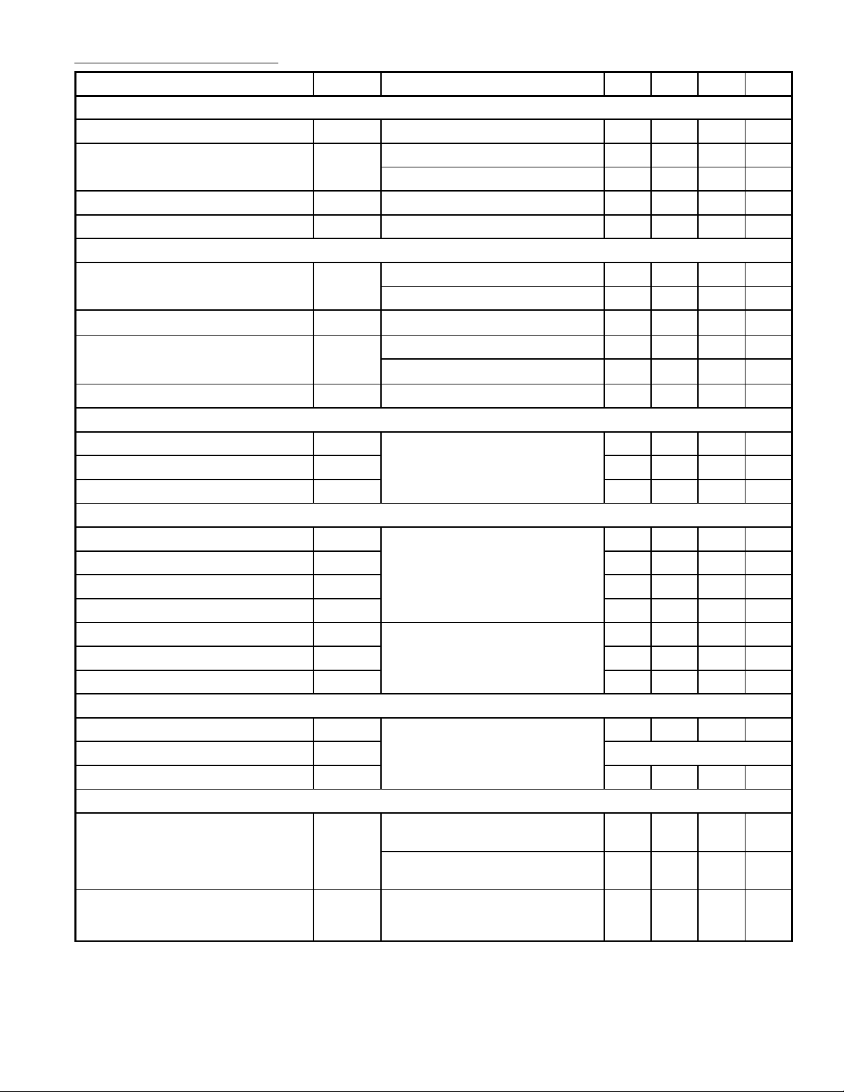
Electrical Characteristics: (TC = +25°C unless otherwise specified)
Parameter Symbol Test Conditions Min Typ Max Unit
OFF Characteristics
Drain–Source Breakdown Voltage V
Zero–Gate Voltage Drain Current I
Gate–Body Leakage Current, Forward I
Gate–Body Leakage Current, Reverse I
(BR)DSSID
DSS
GSSF
GSSR
ON Characteristics (Note 1)
Gate Threshold Voltage V
Static Drain–Source On Resistance r
Drain–Source ON–Voltage V
Forward Transconductance g
GS(th)
DS(on)
DS(on)
fs
Dynamic Characteristics
Input Capactiance C
Output Capacitance C
Reverse Transfer Capactiance C
iss
oss
rss
Switching Characteristics (TJ = +100°C, Note 1)
= 0.25mA, VGS = 0 60 – – V
VGS = 0, VDS = Max Rating – – 0.2 mA
VGS = 0, VDS = 48V, TJ = +125°C – – 1.0 mA
VDS = 0, V
VDS = 0, V
= 20V – – 100 nA
GSF
= 20V – – 100 nA
GSR
VDS = VGS, ID = 1mA 2.0 – 4.5 V
VDS = VGS, ID = 1mA, TJ = +100°C 1.5 – 4.0 V
VGS = 10V, ID = 6A – – 0.2
Ω
VGS = 10V, ID = 12A – – 3.0 V
VGS = 10V, ID = 6A, TJ = 100°C –
–
2.8 V
VDS = 15V, ID = 6A 4 – – mhos
VDS = 25V, VGS = 0,
f = 1MHz
– – 400 pf
– – 300 pf
– – 100 pf
Turn–On Time t
Rise Time t
Turn–Off Delay Time t
Fall Time t
Total Gate Charge Q
Gate–Source Charge Q
Gate–Drain Charge Q
d(on)
r
d(off)
f
g
gs
gd
Source Drain Diode Characteristics (Note 1)
Forward ON Voltage V
Forward Turn–On Time t
Reverse Recovery Time t
SD
on
rr
Internal Package Inductance
Internal Drain Inductance L
Internal Source Inductance L
d
s
VDD = 25V, ID = 0.5 Rated ID,
R
= 50Ω
gen
VDS = 48V, VGS = 10V,
ID = Rated I
D
IS = Rated ID, VGS = 0
Measured from the contact screw
on tab to center of die
Measured from the drain lead 0.25”
from package to center of die
Measured from the source lead
0.25” from package to source bond
pad
– – 60 ns
– – 160 ns
– – 80 ns
– – 110 ns
– 13 26 nC
– 6 – nC
– 7 – nC
– 1.8 3.2 V
Limited by stray inductance
– 300 – ns
– 3.5 – nH
– 4.5 – nH
– 7.5 – nH
Note 1. Pulse test: Pulse width ≤ 300µs, Duty cycle ≤ 2%.
 Loading...