


NTE239
Silicon Controlled Switch (SCS)
Description:
The NTE239 is a silicon controlled switch in a TO72 type package designed for use as a driver for
a numerical indicator tube and switching applications.
Features:
D Selective Breakover Voltage
D Low ON Voltage
Absolute Maximum Ratings:
Collector–Base Voltage, V
(TA = +25°C unless otherwise specified)
CBO
NPN 70V. . . . . . . . . . . . . . . . . . . . . . . . . . . . . . . . . . . . . . . . . . . . . . . . . . . . . . . . . . . . . . . . . . . . . . . .
PNP –70V. . . . . . . . . . . . . . . . . . . . . . . . . . . . . . . . . . . . . . . . . . . . . . . . . . . . . . . . . . . . . . . . . . . . . . .
Collector–Emitter Voltage (NPN Only, R
Collector–Emitter Voltage (PNP), V
Emitter–Base Voltage, V
EBO
CEO
NPN 5V. . . . . . . . . . . . . . . . . . . . . . . . . . . . . . . . . . . . . . . . . . . . . . . . . . . . . . . . . . . . . . . . . . . . . . . . .
PNP –70V. . . . . . . . . . . . . . . . . . . . . . . . . . . . . . . . . . . . . . . . . . . . . . . . . . . . . . . . . . . . . . . . . . . . . . .
Emitter Current, I
E
NPN –100mA. . . . . . . . . . . . . . . . . . . . . . . . . . . . . . . . . . . . . . . . . . . . . . . . . . . . . . . . . . . . . . . . . . . .
PNP 100mA. . . . . . . . . . . . . . . . . . . . . . . . . . . . . . . . . . . . . . . . . . . . . . . . . . . . . . . . . . . . . . . . . . . . .
Peak Emitter Current (t
≤ 1ms, δ = 0.05), I
p
NPN –500mA. . . . . . . . . . . . . . . . . . . . . . . . . . . . . . . . . . . . . . . . . . . . . . . . . . . . . . . . . . . . . . . . . . . .
PNP 500mA. . . . . . . . . . . . . . . . . . . . . . . . . . . . . . . . . . . . . . . . . . . . . . . . . . . . . . . . . . . . . . . . . . . . .
Collector Current (NPN Only), I
C
Continuous 50mA. . . . . . . . . . . . . . . . . . . . . . . . . . . . . . . . . . . . . . . . . . . . . . . . . . . . . . . . . . . . . . . .
Peak 100mA. . . . . . . . . . . . . . . . . . . . . . . . . . . . . . . . . . . . . . . . . . . . . . . . . . . . . . . . . . . . . . . . . . . .
Power Dissipation, P
Operating Junction Temperature, T
Storage Temperature Range, T
D
J
stg
= 10kΩ), V
BE
EM
CER
70V. . . . . . . . . . . . . . . . . . . . . . . . . . . . . . .
–70V. . . . . . . . . . . . . . . . . . . . . . . . . . . . . . . . . . . . . . . . . . . . . . .
250mW. . . . . . . . . . . . . . . . . . . . . . . . . . . . . . . . . . . . . . . . . . . . . . . . . . . . . . . . . .
+150°C. . . . . . . . . . . . . . . . . . . . . . . . . . . . . . . . . . . . . . . . . . . . . . .
–55° to +175°C. . . . . . . . . . . . . . . . . . . . . . . . . . . . . . . . . . . . . . . . . .
Electrical Characteristics: (TA = +25°C unless otherwise specified)
Parameter Symbol Test Conditions Min Typ Max Unit
NPN Transistor
Collector Cutoff Current I
Emitter Cutoff Current I
DC Current Gain h
PNP Transistor
Emitter Cutoff Current –I
DC Current Gain h
Combined Device
Anode–Cathode Voltage V
Holding Current I
Turn–Off Time t
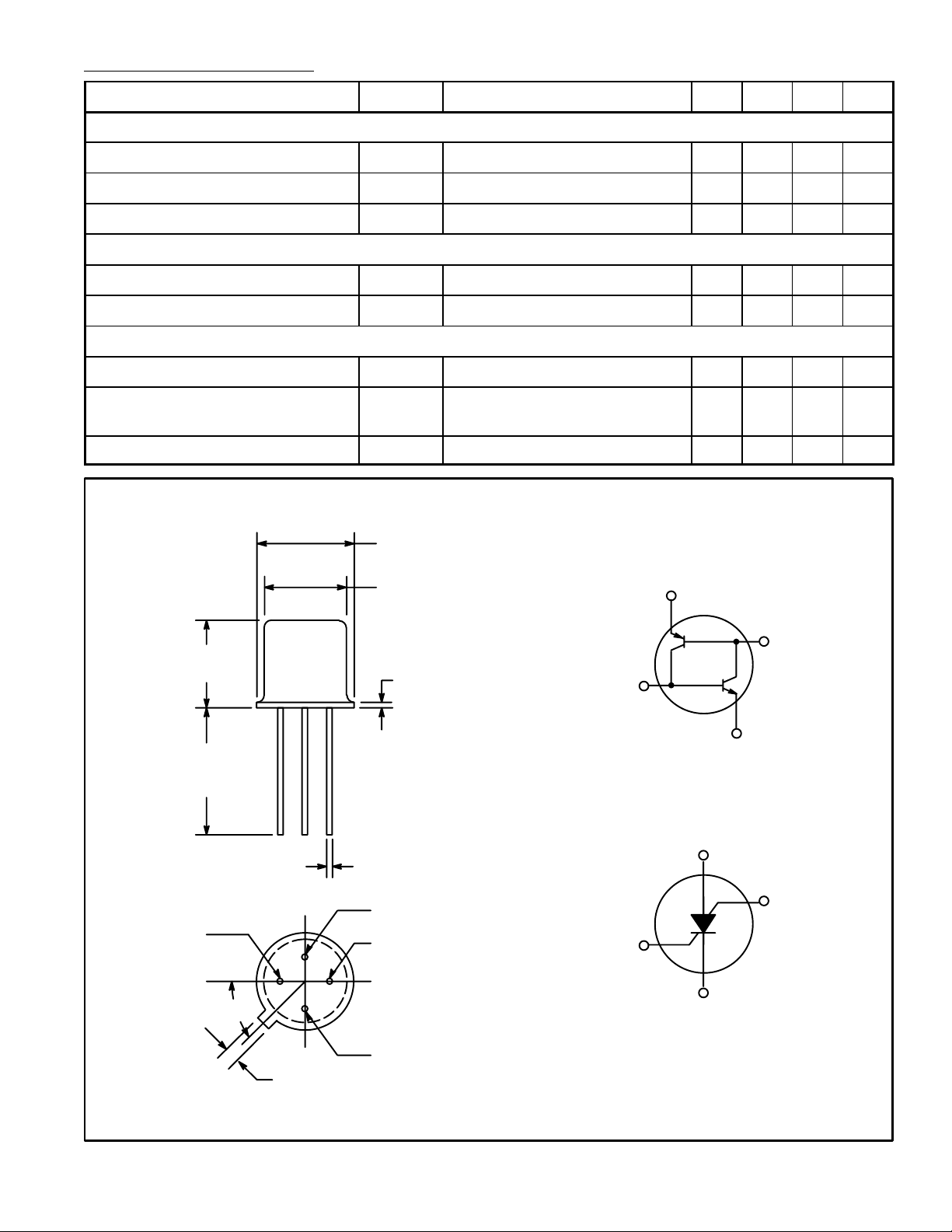
.220 (5.58) Dia
.185 (4.7) Dia
CER
EBO
FE
EBO
FE
AK
H
off
VCE = 70V, RBE = 10kΩ – 10 100 nA
VEB = 5V, IC = 0 – 30 1000 nA
VCE = 2V, IC = 10mA 50 180 –
–VEB = 70V, IC = 0 – 0.05 100 nA
VCB = 0, IE = 1mA 0.72 – 2.5
IA = 50mA, IC = 0, RBE = 10kΩ – 1.05 1.4 V
RBE = 10kΩ, IC = 10mA, –V
BB
0.1 0.5 1.0 mA
= 2V
RBE = 10kΩ – 6 12 µs
4
Emitter (PNP)
.190
(4.82)
.500
(12.7)
Min
.018 (0.45) Dia
1
45°
.040 (1.02)
.030 (.762)
2
3
4
3
Base (PNP)/
Collector (NPN)
2
Collector (PNP)/
Base (NPN)
Emitter (NPN)
1
Transistor Basing
4
Anode
3
Anode/Gate
2
Cathode/Gate
Cathode
1
Thyristor Basing
 Loading...