

NTE NTE2388 Datasheet

NTE2388
MOSFET
N–Channel Enhancement Mode,
High Speed Switch
Description:
The NTE2388 is an N–Channel Enhancement Mode Power MOS Field Effect Transistor in a TO220
type package designed for low voltage, high speed power switching applications such as switching
regulators, converters, solenoid, and relay drivers.
Features:
D Silicon Gate for Fast Switching Speeds
D Low r
DS(on)
D Rugged – SOA is Power Dissipation Limited
D Source–to–Drain Diode Characterized for Use With Inductive Loads
Absolute Maximum Ratings:
Drain–Source Voltage, V
Drain–Gate Voltage (R
Gate–Source Voltage, V
Drain Current, I
Continuous
Peak
Total Power Dissipation (T
Derate Above 25°C 1W/°C. . . . . . . . . . . . . . . . . . . . . . . . . . . . . . . . . . . . . . . . . . . . . . . . . . . . . . . . .
Maximum Operating Junction Temperature Range, T
Storage Temperature Range, T
Maximum Thermal Resistance, Junction–to–Case, R
Maximum Thermal Resistance, Junction–to–Ambient, R
Maximum Lead Temperature (During soldering, 1/8” from case for 5sec), T
to Minimize On–Losses. Specified at Elevated Temperatures.
DSS
= 20kΩ), V
GS
GS
D
T
= +25°C 18A. . . . . . . . . . . . . . . . . . . . . . . . . . . . . . . . . . . . . . . . . . . . . . . . . . . . . . . . . . . . . . .
C
DGR
TC = +100°C11A. . . . . . . . . . . . . . . . . . . . . . . . . . . . . . . . . . . . . . . . . . . . . . . . . . . . . . . . . . . . . .
T
= +25°C 72A. . . . . . . . . . . . . . . . . . . . . . . . . . . . . . . . . . . . . . . . . . . . . . . . . . . . . . . . . . . . . . .
C
= +25°C), P
C
stg
D
J
–55° to +150°C. . . . . . . . . . . . . . . . . . . . . . . . .
–55° to +150°C. . . . . . . . . . . . . . . . . . . . . . . . . . . . . . . . . . . . . . . . . .
thJC
thJA
L
1°C/W. . . . . . . . . . . . . . . . . . . . . . . . . . . . . .
62.5°C/W. . . . . . . . . . . . . . . . . . . . . . . .
+300°C. . . . . . . . . . . .
200V. . . . . . . . . . . . . . . . . . . . . . . . . . . . . . . . . . . . . . . . . . . . . . . . . . . . . . . .
200V. . . . . . . . . . . . . . . . . . . . . . . . . . . . . . . . . . . . . . . . . . . . .
±20V. . . . . . . . . . . . . . . . . . . . . . . . . . . . . . . . . . . . . . . . . . . . . . . . . . . . . . . . .
125W. . . . . . . . . . . . . . . . . . . . . . . . . . . . . . . . . . . . . . . . . . .
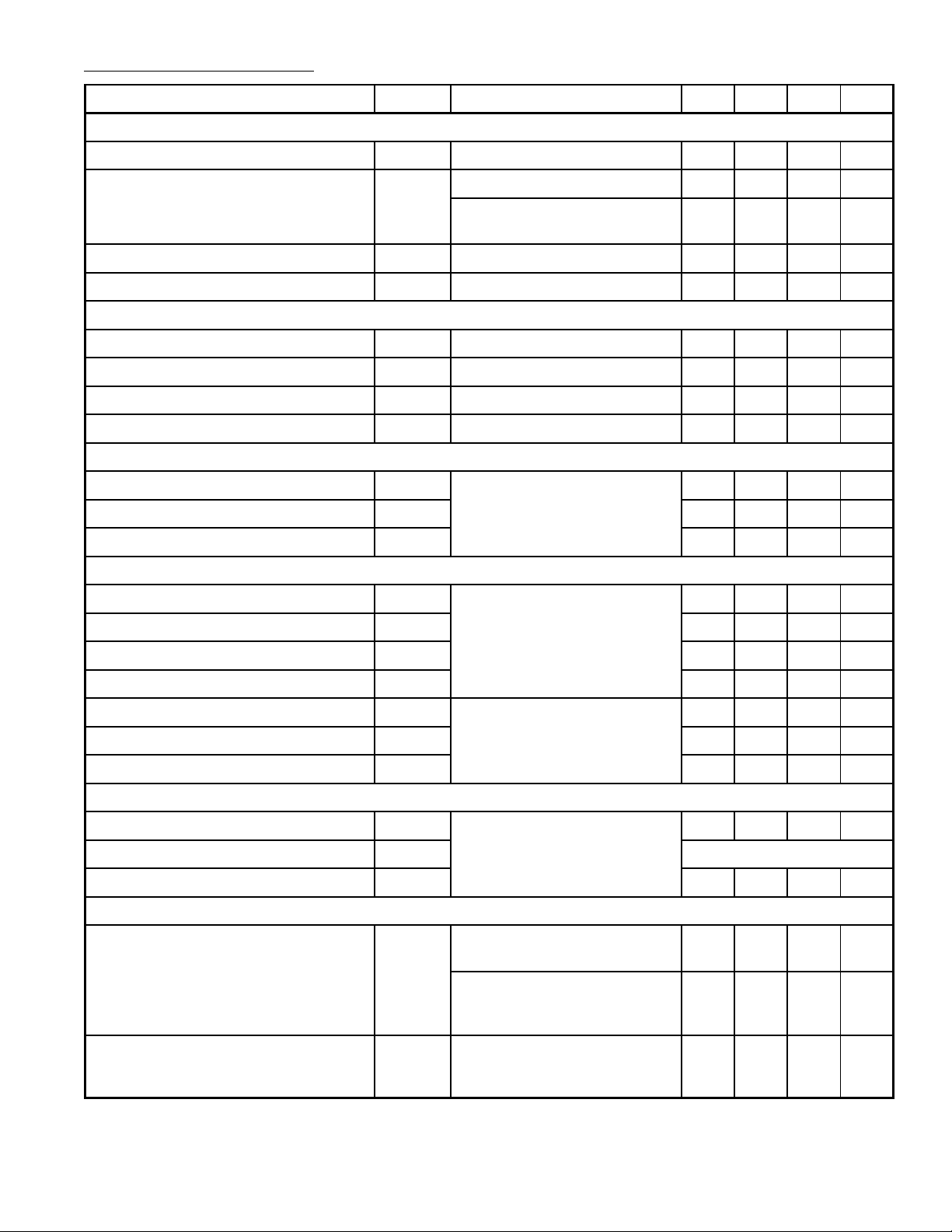
Electrical Characteristics: (TC = +25°C unless otherwise specified)
Parameter Symbol Test Conditions Min Typ Max Unit
OFF Characteristics
Drain–Source Breakdown Voltage V
Zero–Gate Voltage Drain Current I
Gate–Body Leakage Current, Forward I
Gate–Body Leakage Current, Reverse I
(BR)DSSID
DSS
GSSF
GSSR
ON Characteristics (Note 1)
Gate Threshold Voltage V
Static Drain–Source On Resistance R
On–State Drain Current I
Forward Transconductance g
GS(th)
DS(on)VGS
D(on)
fs
Dynamic Characteristics
Input Capactiance C
Output Capacitance C
Reverse Transfer Capactiance C
iss
oss
rss
Switching Characteristics (Note 1)
Turn–On Time t
Rise Time t
Turn–Off Delay Time t
Fall Time t
Total Gate Charge Q
Gate–Source Charge Q
Gate–Drain Charge Q
d(on)
r
d(off)
f
g
gs
gd
Source Drain Diode Characteristics (Note 1)
= 250µA, VGS = 0 200 – – V
VGS = 0, VDS = Max Rating – – 200 µA
VGS = 0, VDS = 160V,
T
= +125°C
C
VDS = 0, V
VDS = 0, V
= 20V – – 100 nA
GSF
= 20V – – 100 nA
GSR
– – 1000 µA
VDS = VGS, ID = 250µA 2 – 4 V
= 10V, ID = 10A – – 0.18 Ω
VGS = 10V, VDS ≥ 3.2V 18 – – A
VDS ≥ 3.2V, ID = 10A 6 – – mhos
VDS = 25V, VGS = 0,
f = 1MHz
– – 1600 pf
– – 750 pf
– – 300 pf
VDD [ 75V, ID = 10A
Rg = 4.7Ω
PEAK
,
– – 30 ns
– – 60 ns
– – 80 ns
– – 60 ns
VDS = 160V, VGS = 10V,
ID = Rated I
D
– 38 60 nC
– 16 – nC
– 22 – nC
Forward ON Voltage V
Forward Turn–On Time t
Reverse Recovery Time t
SD
on
IS = Rated ID, VGS = 0
rr
Internal Package Inductance
Internal Drain Inductance L
Measured from the contact
d
screw on tab to center of die
Measured from the drain lead
0.25” from package to center
of die
Internal Source Inductance L
Measured from the source
s
lead 0.25” from package to
source bond pad
Note 1. Pulse test: Pulse width ≤ 300µs, Duty cycle ≤ 2%.
– 1.8 2.0 V
Limited by stray inductance
– 450 – ns
– 3.5 – nH
– 4.5 – nH
– 7.5 – nH
 Loading...