

NTE NTE2387 Datasheet
NTE2387
MOSFET
N–Channel Enhancement Mode,
High Speed Switch
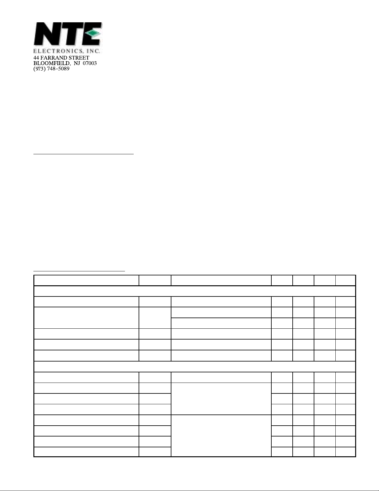
Absolute Maximum Ratings:
Drain–Source Voltage, V
Drain–Gate Voltage (R
Gate–Source Voltage, V
Pulsed Drain Current, I
Continuous Drain Current, I
TC = +25°C 4.0A. . . . . . . . . . . . . . . . . . . . . . . . . . . . . . . . . . . . . . . . . . . . . . . . . . . . . . . . . . . . . . . . .
= +100°C 2.5A. . . . . . . . . . . . . . . . . . . . . . . . . . . . . . . . . . . . . . . . . . . . . . . . . . . . . . . . . . . . . . . .
T
C
Total Dissipation (T
Operating Junction Temperature, T
Storage Temperature Range, T
Maximum Thermal Resistance, Junction–to–Case, R
Typical Thermal Resistance, Junction–to–Ambient, R
DS
= 20kΩ), V
GS
GS
DM
D
= +25°C), P
C
DGR
tot
J
stg
thJC
thJA
800V. . . . . . . . . . . . . . . . . . . . . . . . . . . . . . . . . . . . . . . . . . . . . . . . . . . . . . . . .
800V. . . . . . . . . . . . . . . . . . . . . . . . . . . . . . . . . . . . . . . . . . . . .
±30V. . . . . . . . . . . . . . . . . . . . . . . . . . . . . . . . . . . . . . . . . . . . . . . . . . . . . . . . .
16A. . . . . . . . . . . . . . . . . . . . . . . . . . . . . . . . . . . . . . . . . . . . . . . . . . . . . . . . . . .
125W. . . . . . . . . . . . . . . . . . . . . . . . . . . . . . . . . . . . . . . . . . . . . . . . .
+150°C. . . . . . . . . . . . . . . . . . . . . . . . . . . . . . . . . . . . . . . . . . . . . . .
–55° to +150°C. . . . . . . . . . . . . . . . . . . . . . . . . . . . . . . . . . . . . . . . . .
1.0°C/W. . . . . . . . . . . . . . . . . . . . . . . . . . . .
60°C/W. . . . . . . . . . . . . . . . . . . . . . . . . . . .
Electrical Characteristics:
Parameter Symbol Test Conditions Min Typ Max Unit
Static Characteristics
Drain–Source Breakdown Voltage V
Zero–Gate Voltage Drain Current I
Gate–Body Leakage Current I
Gate Threshold Voltage V
Static Drain–Source On Resistance R
Dynamic Characteristics
Forward Transconductance g
Input Capactiance C
Output Capacitance C
Reverse Transfer Capactiance C
Turn–On Time t
Rise Time t
Turn–Off Delay Time t
Fall Time t
(TC = +25°C unless otherwise specified)
(BR)DSSID
DSS
GSS
GS(th)
DS(on)VGS
iss
oss
rss
d(on)
d(off)
VGS = 0, VDS = 800V, TC = +25°C – 2 20 µA
VGS = 0, VDS = 800V, TC = +125°C – 0.1 1.0 mA
VDS = 0, VGS = ±30V – 10 100 nA
VDS = VGS, ID = 1mA 2.1 3.0 4.0 V
VDS = 25V, ID = 1.5A 3.0 4.3 – mho
fs
VDS = 25V, VGS = 0, f = 1MHz
VDD = 30V, ID = 2.3A, VGS = 10V,
RGS = 50Ω, R
r
f
= 250µA, VGS = 0 800 – – V
= 10V, ID = 1.5A – 2.7 3.0
– 1000 1250 pf
– 80 120 pf
– 30 50 pf
– 10 25 ns
= 50Ω
gen
– 25 40 ns
– 130 150 ns
– 40 60 ns
Ω
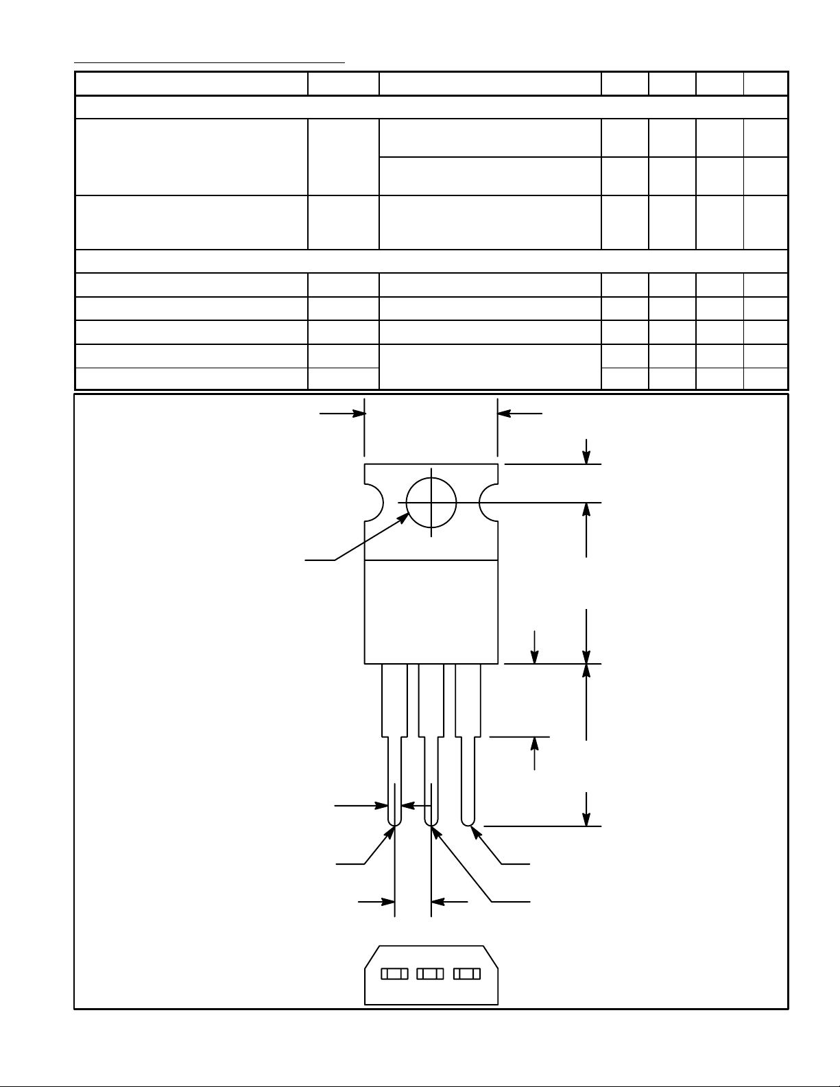
Electrical Characteristics (Cont’d): (TC = +25°C unless otherwise specified)
Parameter Symbol Test Conditions Min Typ Max Unit
Dynamic Characteristics (Cont’d)
Internal Drain Inductance L
Internal Source Inductance L
Source–Drain Diode Ratings and Characteristics
Continuous Reverse Drain Current I
Pulsed Reverse Drain Current I
Diode Forward Voltage V
Reverse Recovery Time t
Reverse Recovered Charge Q
DR
DRM
SD
rr
Measured from contact screw on tab
D
to center of die
Measured from drain lead 6mm from
package to center of die
Measured from the source lead
S
6mm from package to source
bonding pad
IF = 4A, VGS = 0 – 1.0 1.3 V
IF = 4A, diF/dt = 100A/µs, VGS = 0,
VR = 100V
rr
– 3.5 – nH
– 4.5 – nH
– 7.5 – nH
– – 4 A
– – 16 A
– 1800 – ns
– 12 – µC
.420 (10.67)
Max
.110 (2.79)
.147 (3.75) Dia Max
.070 (1.78) Max
.100 (2.54)
Gate
.500
(12.7)
Max
.250 (6.35)
Max
.500
(12.7)
Min
Source
Drain/Tab
 Loading...