

NTE NTE2384 Datasheet
NTE2384
MOSFET
N–Channel Enhancement Mode,
High Speed Switch
Absolute Maximum Ratings:
Drain–Source Voltage, V
Drain–Gate Voltage (R
Gate–Source Voltage, V
Pulsed Drain Current (T
Continuous Drain Current, I
TC = +30°C 6.0A. . . . . . . . . . . . . . . . . . . . . . . . . . . . . . . . . . . . . . . . . . . . . . . . . . . . . . . . . . . . . . . . .
= +100°C 3.9A. . . . . . . . . . . . . . . . . . . . . . . . . . . . . . . . . . . . . . . . . . . . . . . . . . . . . . . . . . . . . . . .
T
C
Total Dissipation (T
Operating Junction Temperature, T
Storage Temperature Range, T
Maximum Thermal Resistance, Junction–to–Case, R
Typical Thermal Resistance, Junction–to–Ambient, R
DS
= 20kΩ), V
GS
GS
= +25°C), I
C
D
= +25°C), P
C
DGR
DM
tot
J
stg
thJC
thJA
800V. . . . . . . . . . . . . . . . . . . . . . . . . . . . . . . . . . . . . . . . . . . . . . . . . . . . . . . . .
800V. . . . . . . . . . . . . . . . . . . . . . . . . . . . . . . . . . . . . . . . . . . . .
±20V. . . . . . . . . . . . . . . . . . . . . . . . . . . . . . . . . . . . . . . . . . . . . . . . . . . . . . . . .
24A. . . . . . . . . . . . . . . . . . . . . . . . . . . . . . . . . . . . . . . . . . . . . . .
125W. . . . . . . . . . . . . . . . . . . . . . . . . . . . . . . . . . . . . . . . . . . . . . . . .
+150°C. . . . . . . . . . . . . . . . . . . . . . . . . . . . . . . . . . . . . . . . . . . . . . .
–55° to +150°C. . . . . . . . . . . . . . . . . . . . . . . . . . . . . . . . . . . . . . . . . .
1.0°C/W. . . . . . . . . . . . . . . . . . . . . . . . . . . .
35°C/W. . . . . . . . . . . . . . . . . . . . . . . . . . . .
Electrical Characteristics:
Parameter Symbol Test Conditions Min Typ Max Unit
Static Characteristics
Drain–Source Breakdown Voltage V
Zero–Gate Voltage Drain Current I
Gate–Body Leakage Current I
Gate Threshold Voltage V
Static Drain–Source On Resistance R
Dynamic Characteristics
Forward Transconductance g
Input Capactiance C
Output Capacitance C
Reverse Transfer Capactiance C
Turn–On Time t
Rise Time t
Turn–Off Delay Time t
Fall Time t
(TC = +25°C unless otherwise specified)
(BR)DSSID
DSS
GSS
GS(th)
DS(on)VGS
iss
oss
rss
d(on)
d(off)
VGS = 0, VDS = 800V, TJ = +25°C – 20 250 µA
VGS = 0, VDS = 800V, TJ = +125°C – 0.1 1.0 mA
VDS = 0, VGS = ±20V – 10 100 nA
VDS = VGS, ID = 1mA 2.1 3.0 4.0 V
VDS = 25V, ID = 3A 1.8 3.0 – mho
fs
VDS = 25V, VGS = 0, f = 1MHz
VDD = 30V, ID = 2.6A, VGS = 10V,
RGS = 50Ω, R
r
f
= 250µA, VGS = 0 800 – – V
= 10V, ID = 3A – 1.3 1.5
– 3900 5000 pf
– 200 350 pf
– 80 140 pf
– 60 90 ns
= 50Ω
gen
– 90 140 ns
– 330 430 ns
– 110 140 ns
Ω
Electrical Characteristics (Cont’d): (TC = +25°C unless otherwise specified)
Parameter Symbol Test Conditions Min Typ Max Unit
Dynamic Characteristics (Cont’d)
Internal Drain Inductance L
Internal Source Inductance L
Source–Drain Diode Ratings and Characteristics
Continuous Reverse Drain Current I
Pulsed Reverse Drain Current I
Diode Forward Voltage V
Reverse Recovery Time t
Reverse Recovered Charge Q
DR
DRM
SD
rr
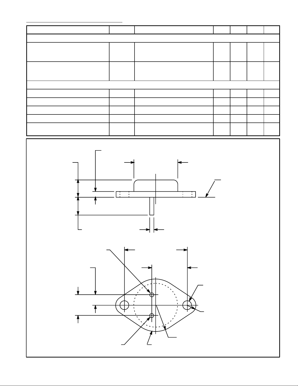
Measured from contact screw on
D
header closer to source pin and
center of die
Measured from the source lead
S
6mm from package to source
bonding pad
TC = +25°C – – 6 A
TC = +25°C – – 24 A
IF = 12A, VGS = 0, TJ = +25°C – 1.1 1.5 V
IF = 6A, TJ = +25°C – 1800 – ns
VGS = 0, VR = 100V, TJ = +25°C,
rr
di
.135 (3.45) Max
.350 (8.89)
/dt = 100A/µs,
F
.875 (22.2)
Dia Max
– 5.0 – nH
– 12.5 – nH
– 25 – µC
Seating
Plane
.215 (5.45)
.430
(10.92)
Source
.040 (1.02).312 (7.93) Min
1.187 (30.16)
.665
(16.9)
.156 (3.96) Dia
(2 Holes)
.188 (4.8) R Max
.525 (13.35) R Max
Drain/CaseGate
 Loading...